LPPN step-down type. The simplest way direct conversion of direct voltage consists of periodic switching of the collector current in a circuit connected to a constant voltage source (Fig. 6.3, a) using a key element - a power transistor VT 1. In powerful low-frequency converters of this type Load current switching is carried out using thyristors. The operation of the valve elements in the switching mode makes it possible to ensure the efficiency of such a converter is close to unity.
For NPPN there are two operating modes. The first mode is characterized by the fact that by the time the switch is closed again (opening a powerful transistor or thyristor), a certain minimum current flows in the inductor - i Lmin(Fig. 6.3, b). This mode is called “continuous current mode”. It is also characterized by the least internal resistance converter and is therefore preferred.
Figure 6.3 - Direct DC-DC converter
step-down type:
A - electrical diagram; b, c, d – time diagrams of currents
During the time interval of the open state of the transistor ( t-t 0) collector current i 0 repeats the shape of the current in the inductor, and during the time interval t=t h, when the transistor is closed, the current i 0 is equal to zero.
The second mode is called “intermittent current mode”. It occurs at relatively small loads (the resistance of the resistor is high R n) converter, when the current in the filter choke manages to decrease to zero before the next opening of the powerful transistor occurs VT 1.
In the future, we will consider the operation of various LPPN circuits in the continuous current mode and periodic closing and opening of the switch with a pulse repetition period T.
Using the control system, changing the ratio between the durations of the open t 0 and closed t 3 (Fig. 6.3, b) states of the transistor in the power circuit of the LPPN, it is possible to obtain different levels of the average voltage across the load. In this mode of use, these converter devices are often called switching regulators in practice.
With the key closed (transistor VT 1 is open) at the filter input the voltage is equal to the voltage U n power source. This voltage forms a voltage pulse at the receiver U n = U n, and pulse duration t and is equal to the time the transistor is open ( t 0 =t And).
With the key open (transistor VT 1 is locked) the voltage at the receiver is zero. Since the pulses follow with a period T, then the time interval of the closed state of the transistor is equal to t z = T-t O.
The average voltage value at the receiver over a period according to (6.1) is directly proportional to the duty cycle To h.
 .
.
The output voltage of the PPN is the average value of the voltage across the load
U n = U avg = U p × To h. (6.3)
Accordingly, the voltage transfer coefficient for this circuit has the form
 (6.4)
(6.4)
And tension U n, and transmission coefficient U n/ U n are directly proportional to the relative duration of the pulses.
If the circuit did not have a branch with a blocking diode VD 1, then when the key is opened (the transistor is locked VT 1) a significant off-design back-EMF would be induced at the throttle e L= - L× di/dt, which could either lead to a breakdown of the inductor winding insulation, or to an electric arc at the point of the circuit break (on the key, i.e. on the emitter-collector R-n transistor transition VT 1) and to failure of either the inductor or the transistor.
In a circuit with a diode, at the beginning of the process of increasing this EMF, a negative voltage appears at the cathode of the diode, it opens, which allows the inductor to discharge through the resistance of the receiver and the filter capacitor. Inductor current during interval t 0 passes through the source, and during the interval t 3 - through a diode VD 1 (Fig. 6.3, c, d).
Expression (6.4) determines the control characteristic of the LPPN shown in Fig. 6.3a, in the power circuit of which a filter choke is connected in series L and the key is a transistor VT 1. From (6.4) it follows that with increasing Toз transmission coefficient LPPN changes linearly (see Fig. 6.6) from zero (at t 0 = 0) to unity (with t 0 = T). The circuit discussed above makes it possible to obtain a load voltage equal to or less than the supply voltage, i.e. U n £ U p. Therefore, such an LPPN is sometimes called a buck-type converter.
Along with the type of LPPN considered above with a series connection with a receiver of a power transistor and a filter choke, other LPPNs of the step-down type are also used in practice (albeit much less frequently), differing from each other in the configuration of the power circuits.
LPPN step-up type. The second option for connecting the elements of the power circuit in the PPN is a circuit with the inductor switched on in series with the receiver and the switch switched on in parallel (Fig. 6.4, a).
From the moment the key opens (transistor closes VT 1) in the time interval of the closed state of the transistor t h the current begins to decline i L in the inductor, the derivative of the current changes its sign and a back-EMF is induced in the inductor winding e dr = L× di/dt, preventing the decrease in current in the inductor and directed in the direction of the current. The voltage on the inductor that balances this EMF is u dr =- e dr is summed with the voltage of the power source and at the emitter-collector junction of the transistor VT 1 total voltage U e-k = U n + u dr increases.
Diode VD 1 opens and capacitor WITH starts charging again (Fig. 6.4,b). Voltage U eq on a closed transistor is equal to the output voltage U n converter.
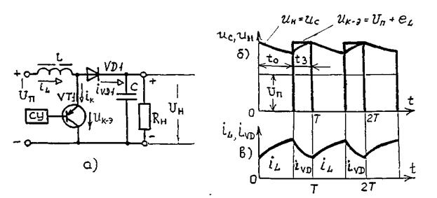
Figure 6.4 - Direct DC-DC converter
boost type:
a – diagram; b – time diagrams of currents and voltages
The energy stored in the inductor is transferred to the capacitor WITH and resistor R n through the opened diode VD 1. The current in the inductor decreases, reaching its minimum value at the end of this interval.
To determine the transmission ratio U n/ U n this PPN circuit, we introduce the assumption that the inductance of the inductor L is a very large value, close to L=¥.
In this case, the time constants of the charge-discharge circuits of the inductor are large, the process of increasing and decreasing the current in the inductor is very long and over the interval of the pulse repetition period T current changes are negligible. You can take the average values of charge-discharge currents equal and unchanged, i.e. count I L.sar.sr = I L.res.sr = I L=const. With these assumptions, it is possible to draw up a balance of energies of the power source when charging and discharging the inductor within the period T(neglecting losses).
The energy supplied to the circuit by the power source over the entire pulse period T=t 0 +t h, is partially stored in the inductor (in the time interval of the open state of the transistor), and in the time interval t h, corresponding to the closed state of the transistor, is partially used to recharge the capacitor and is partially consumed in the load resistor R n. The source energy equation for a period has the form
W and = U p × I L× T.(6.5)
On the other hand, we can write the equation for the same source energy W and ¢, given to the circuit in the amount of energy accumulated in the inductor in the time interval of the closed state of the transistor t h.
To compile such an equation with equal amounts of energy released by the source into the external circuit in both cases ( W and = W¢ i), it must be assumed that the source voltage is in the range t z is no longer equal U p, and other: U n = U n + u etc., where U dr – additional voltage on the inductor, equivalent to the previously considered back-EMF in the inductor winding
W and ¢ = U n × I L× t з =U n × I L×( T-t 0). (6.6)
Equating expressions (6.5) and (6.6), we obtain
 (6.7)
(6.7)
From expression (6.7) you can determine the transmission coefficient of the considered LPPN, having previously divided the right side into T:
![]() . (6.8)
. (6.8)
Graphical dependence of the transmission coefficient of such a PPN circuit shown in Fig. 6.4 is shown in Fig. 6.6.
Thus, in an LPPN with such a power circuit, the output voltage is always greater than the input voltage. This happens because during the inductor discharge stage, both the energy stored in the inductor and the energy of the power source enter the load. The transmission coefficient of this circuit varies from 1 at K z =0 to infinity at K z =1. Such NPPNs are often called boost converters.
LPPN inverting type. The third type of NPPN is shown in Fig. 6.5, a. Its power circuit is formed by a transistor connected in series with the load and a choke connected in parallel to it.
"Documentation" - Technical information by application electronic components, features of construction of various radio engineering And electronic circuits , as well as documentation on the features of working with engineering software and regulatory documents (GOST).
Step-up DC-DC voltage converters (Step-Up Voltage Converter, Step-Up Voltage Regulator, Boost Converter, PvP) have the peculiarity that the output voltage V 0 of these converters is greater than the input unstabilized voltage V IN . In addition, V 0 is stable when changing V IN and the output current I 0 of the converter. This circumstance determines the use of PvP for powering with a stabilized voltage mainly battery-powered electronic equipment (the input voltage in this case is small) or some units of such equipment, the power supply of which requires a higher voltage than the rest.
The article discusses the operating principle of PvP and describes integrated circuits for the implementation of such converters along with their main electrical parameters. As a rule, such PvP provide positive V 0 .
Principle of operation
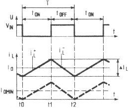
The basic PvP scheme is shown in Fig. 1 a. Switch S is a bipolar transistor n-p-n structures or MOS transistor. The time interval during which the transistor is open (the key is closed, segment t 0N in Fig. 1b) and the interval when the transistor is closed (the key is open, segment t 0FF) are determined by the CON control circuit. When the switch is closed (moments t 0 and t 2 in Fig. 1.b), the voltage at the connection point between the diode VD and the coil L is zero (U = 0), if we neglect the voltage drop across S and Rs. The diode VD is closed due to the positive value of the output voltage, supported by the charge accumulated in the capacitor C. The input voltage V IN is applied to the coil L, and a linearly increasing current flows through it and S
due to which energy is accumulated in the coil magnetic field. During time t ON, the current in the coil increases by the amount:
![]()

Rice. 1.a Basic PvP scheme
In this case, the charged capacitor C provides the output current Io of the circuit. When S opens (moment t 1 in Fig. 1b), the polarity of the voltage applied to L changes its direction and becomes as shown in Fig. 1a. This voltage is added to V IN, providing the ratio U > Vo and the opening of the diode VD. The external voltage applied to L, equal to V IN - Vo, determines the current passing through it:
![]()
Its value decreases linearly over time, because the coil gives up its energy to maintain the current I 0 and restore the charge C. During the time t 0FF, only part of the accumulated energy is given off, so the change in current is (taking into account the ratio of the values of V IN and Vo)
![]()
The minus sign in the superscript of the current indicates that this current flows by expending the energy of the coil. Based on the obvious relation
which takes place in the steady state of operation, we obtain the dependence:
 | (1) |
From this it is clear that Vo > V IN is always, i.e. The scheme is PvP. Normally C ON sets constant frequency
![]()
UCON pulses controlling S. In this case, Vo can be changed by varying t 0FF, which means pulse-width modulation (PWM). Moreover, any undesirable change in Vo leads to such a change in t 0FF that it is restored original value Vo. Thus, the work of PvP as a stabilizer is ensured by C ON through a continuous change in the duty factor (Duty Factor):
control impulses. Expression (1) is often written as
Rice. 1. b Timing diagrams explaining the principle of operation
During PvP operation, current surges i L may occur due to a sharp change in V IN or load resistance at the output, which can lead, even in a short time, to unwanted saturation of the coil. This can be avoided by using current PWM, in which CON regulates the current through the closed contacts S, for which the resistor Rs is used, shown in Fig. 1a with a dotted line. Less commonly used are PvPs with pulse-frequency modulation (PFM, Pulse-Frequency Modulation, PFM), in which fo and δ change simultaneously.
The current i L has a direct component l 0, which is the output current of the PvP, and an undesirable variable component ΔI L, almost completely passing through the capacitor C. For normal operation PvP is recommended to ensure the ratio ΔI L =0.4 I 0 . The remaining small portion of ΔI L passes through the load. This means that the output voltage Vo has a variable component. This is a serious disadvantage of PvP, which limits their use in electronic equipment that provides amplification of weak signals.
A decrease in I O means the accumulation in L and, accordingly, the release of less energy to the load. At I omin = 0.5·ΔI L (dashed line in Fig. 1.b), the accumulated energy and I L become equal to 0 at the moment the switch S is closed. Further reduction of i O is not recommended, although this mode of operation is, in principle, possible . In order to avoid an operating mode in which i 0
An important feature of PvP is that the current I IN consumed from the source V IN is greater than io and has the value
| (2) |
Where &????; - coefficient useful action(efficiency) PvP.
PvP Control Schemes
They have similar circuit designs and operating principles as PnP.
PvP Integrated Circuits
The generalized structure of the IS for PvP is shown in Fig. 2a along with external elements that need to be connected to it. The dotted line indicates connections used only in some ICs. All IC stages are powered by an internal VR regulator. The output voltage Vo is fed to the input feedback FB. Thanks to the divider R1-R2, a certain part of it is supplied to the inverting input of the error amplifier EA. The reference voltage VREF (about 1.25 V) from the REF source is applied to the non-inverting input of this amplifier. In some ICs it is output to a separate pin. A capacitor of about 10 nF is connected between it and ground to prevent external noise from penetrating the non-inverting input of the error amplifier. There are PvP ICs in which stable operation of the error amplifier requires connecting an external RC circuit to its output (COMP compensation pin). Enhanced EA difference
![]()
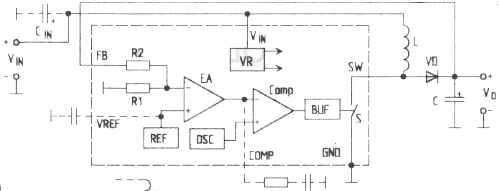
Rice. 2.a. IP for PVP
is compared by comparator Comp with a fixed-frequency ramp voltage fo generated by the built-in OSC oscillator. The result of this comparison is PWM pulses at the output of the comparator, which drive the switch S through the buffer BUF. In some ICs, the key S is installed outside the circuit. In this case, the SW pin is the BUF output (Fig. 2.b). Quite rarely, a VD diode is a structural element of an IC (Fig. 2.c).
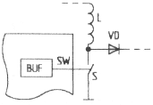
Rice. 2.b. The SW pin is the BUF output
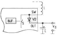
Rice. 2. c. Sometimes the VD diode is a structural element of the IC
The circuit shown in Fig. 2a is designed for a fixed output voltage Vo. There are VOPs with variable Vo, in which R1-R2 are an external divider, and the FB pin is directly connected to the inverting input of the error amplifier.
One of the ever-expanding areas of PvP application is equipment powered by a single battery (Single-Cell Instruments). This is an alkaline or nickel-cadmium cell with a voltage of 1.15...1.56 V or a lithium cell with a voltage of 2.30...3.10 V. Since this requires that the IC operate normally up to a supply voltage V IN = 1 V, it has a different design, shown in Fig. 2.d. The voltage V IN through the filter coil Lo (its inductance is several millihenries) powers only the OSC generator. At its additional output it creates a fairly high alternating voltage, which is converted to direct voltage by the REC rectifier unit. The resulting DC voltage V+, typically 12V, is filtered by an external capacitor C of about 1uF and stabilized by VR, which in turn powers the rest of the IC.>
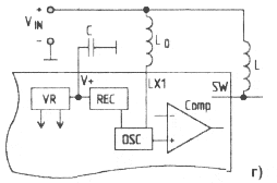
Rice. 2. d. PnP design, running on one battery
Table 1
| Micro type scheme | Module type lations | Vo,V | Iomax,A | Efficiency,% | fo,kHz | V IN ,V | LR | LdR | VREF,B |
| LM2577 | PWM | 12; 15; 5..50 | 3 | 80 | 52 | 3,5..40 | 20mV | 20mV | 1,23 |
| LM2587 | PWM | 3,3; 5,0; 12; 5..50 | 5 | 75 | 100 | 4..40 | 20 mV | 20 mV | 1,23 |
| MAX654 | PWM | 5 | 0,04 | - | 18 | 1,15..1,56 | - | - | 1,25 |
| MAX655 | PWM | 5 | 0,06 | - | 18 | 2,30..3,10 | - | - | 1,25 |
| MAX657 | PWM | 3 | 0,06 | - | 18 | 1,15..1,56 | - | - | 1,25 |
| MAX659 | PWM | 3 | 0,06 | - | 18 | 2,30..3,10 | - | - | 1,25 |
| MAX731 | TSHIM | 5 | 0,2 | 82...87 | 170 | 2,5...5,52 | 0.2%/V | 0.005%/mA | 1,23 |
| MAX732 | TSHIM | 12 | 0,2 | 82...92 | 170 | 4,0..9,3 | 0.2%/V | 0.0035%/mA | 1,23 |
| MAX733 | TSHIM | 15 | 0,125 | 82..92 | 170 | 4,0..9,3 | 0.2%/V | 0.0035%/mA | 1,23 |
| MAX734 | TSHIM | 12 | 0,12 | 85 | 170 | 4,0..11,0 | 0.2%/V | 0.0035%/mA | 1,23 |
| MAX751 | TSHIM | 5 | 0,15 | 86 | 170 | 2,7..5,0 | 0.2%/V | 0.005%/mA | 1,23 |
| MAX752 | TSHIM | 1,8..15 | 0,2 | 85..95 | 170 | 1,8..11,0 | 0.2%/V | 0.0035%/mA | 1,23 |
| MAX756 | CHIM | 3,3;5 | 0,2 | 87 | 1,8..5,6 | - | - | 1,25 | |
| MAX777 | CHIM | 5 | 0,24 | 85 | 1,0..6,2 | - | - | - | |
| MAX778 | CHIM | 3,0;3,3 | 0,24 | 85 | 1,0..6,2 | - | - | - | |
| MAX779 | CHIM | 1..6 | 0,24 | 85 | 1,0..6,2 | - | - | - |
Main settings
They coincide with the parameters of the buck converters discussed in. The exception is the natural absence of the parameter (V IN - V 0)min, but instead the value of the minimum difference between the input and output voltages is given.
The table shows the main parameters of PvP ICs from two of the world's largest manufacturers, and also indicates the type of modulation used. Here LM are products from National Semiconductor, MAX are circuits from MAXIM.
Rice. 3 Pinout of the ICs given in Table 1
For PvP with PFM, the minimum time interval t OFF MIN, during which the key is closed, and the maximum time interval t 0N max - during which the key is open, are given as parameters. The pinout of the ICs given in the table is given in Fig. Z.
Literature
- Kutsarov, S. Step-down DC-to-DC converters. - Radiomir, 2003, N 7.
- Kutsarov, S. Application of buck converters. - Radiomir, 2003, N 10.
Publication date: 15.03.2004
Readers' opinions
- Vovan / 08.11.2012 - 16:50
I also have an ant. So the charge is probably a little higher than a thousand, somewhere around 1500-1800. Check the brushes, adjust the relay/install an electronic one - Vovan / 02.25.2011 - 18:11
I have a sunrise with an ant motor. The motor design uses a ds 1a dynastarter. Required voltage it gives after 3000 rpm. Due to the peculiarities of operation (driving at a speed of 40 km/h), the battery is almost not charged. I use a regulator relay from a VAZ 2106. I decided to plug in a boost converter between the relay and the exciter winding of the generator. What do you recommend? - Sergey / 02/04/2010 - 20:27
need a circuit 12-24v 12-220v
The increase in electrical loads in the traction power supply system, caused by an increase in the volume of work performed, brought the DC traction power supply systems to their maximum operating modes, without satisfying the required traffic volumes. In this regard, alternative traction systems began to be intensively studied, in addition to systems with a voltage level in the contact network from 6 to 24 kV. These systems require the use of a fundamentally new electric rolling stock, which has on board a controlled converter that lowers the contact network voltage to a level of 1500 V.
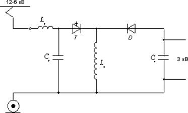
Another solution is a three-wire T.P. system. Tretyak. Its essence lies in the fact that the voltage level in the direct current contact network remains the same, which makes it possible to operate the same electric rolling stock, but a significant part of the electricity is supplied to it with an increased direct current voltage of 6 kV using an additional wire suspended from the field side. The conversion of high-voltage direct current energy into 3 kV direct current energy is carried out by converters located along the electrical railway track. A diagram of such a system is shown in Fig. 1.
Rice. 1. Traction power supply system T.P. Tretyak. CT traction transformers;. I-inverter; EPS - electric rolling stock; NV - neutral insert that separates the contact network into separate sections
Currently, traction drives using asynchronous electric motors are considered promising, the advantages of which have been confirmed by operating experience on European railways. This is facilitated by advances in the creation of turn-on thyristors (GTO and IGCT) and insulated gate bipolar transistors (IGBT) for an operating voltage of 6 kV, used by Siemens, Adtranz and others.
A 15 kV DC electric traction system was proposed in the USA about four decades ago. In Italy, 12 kV DC traction systems have been developed, a comparison has been made between 12 kV DC and 25 kV, 50 Hz AC traction systems in terms of overall capital costs, and it has been proven that they are less for a DC system.
Rice. 2. Possible circuit diagram high-voltage DC electric rolling stock (electric locomotive with pulse control of the traction motor)
The essence of the system is that energy is supplied to the engine using thyristors not continuously, but in portions (pulses). Depending on the pulse duration and frequency, the average voltage on the motor will change. Such regulation is carried out using a thyristor controlled by a special circuit (Fig. 2).
Based on pulse converters, a device called an inverter can be built, which can output both direct (rectified) current and alternating current with an adjustable frequency. The latter circumstance allows the use of very reliable and easy-to-use asynchronous motors as traction motors.
The diagram shown in Fig. 29 works as follows. In the open state of thyristor T, the mains current is closed through the inductor Lg; in the closed state of the thyristor, the current is closed through diode D and the inverter elements. The capacitor C maintains a constant voltage with a variable component depending on the capacitance of the capacitor. In the event of a breakdown of the thyristor, the emergency current is closed through the inductor Lg. The rate of current rise is limited by the inductance of the inductor, which creates favorable conditions for disconnecting the circuit by a protective device (switch). Diode D, with sufficient voltage reserve, protects the inverter from contact with high potential. The above circuit provides the effect of galvanic isolation of the high and low voltage links.
The high-voltage DC electric traction system eliminates the traditional problems of an AC system: reduced power factor, asymmetry of the primary mains voltage and the presence of higher harmonics.