Intel has produced the first prototype processors containing new very small transistors and based on 45nm manufacturing technology, thus accelerating the era of multi-core computing.
Intel Corporation has announced one of the most significant advances in the fundamental principles of transistor design. It was announced that Intel is already using two completely new materials to create insulating walls and logic gates of transistors based on a 45-nanometer manufacturing process. The next-generation multi-core processor families of the next generation Intel® Core™ 2 Duo, Intel® Core™ 2 Quad, and Intel® Xeon® processors will contain hundreds of millions of these microscopic transistors, or electronic switches. Intel also said it already has working prototypes of five processors out of 15 of its future products, which are planned to be released using the new 45-nanometer production technology.
The use of new transistors will allow desktop, laptop and server processors to reach new levels of performance while significantly reducing leakage current. New technology will not only reduce the size of processors, but also reduce power consumption, noise level and cost of the PC. This fundamental technological breakthrough by Intel also builds confidence that Moore's Law, the technology industry's adage that states that the number of transistors on a chip roughly doubles every two years, will hold true well into the next decade.
Intel Corporation experts are confident that the creation of the first workable prototypes of processors manufactured using 45-nanometer technology allowed us to outstrip other players from the semiconductor industry by more than a year. These new Intel processors are part of the next-generation 45nm product family codenamed Penryn. Prototype processors are built for five different segments of the computer market and have been successfully tested with Windows* Vista*, Mac OS X*, Windows* XP and Linux, as well as various applications. As previously planned, Intel Corporation intends to begin mass production of products based on 45-nanometer manufacturing technology in the second half of this year.
New Intel Transistors: Using High-k Material and Metals Based on 45nm Manufacturing Process
Intel is the first in the industry to use an innovative combination of new materials that can significantly reduce transistor leakage current and improve transistor performance in its 45nm manufacturing technology. A new material called high-k is used to create the transistor gate dielectric, and a new combination of metal materials is used for the transistor gate electrode.
“The introduction of new materials such as high-k and metal marks the biggest change in transistor technology since the late 1960s, with the advent of polysilicon gate MOSFETs,” said Gordon Moore, one of the co-founders of Intel Corporation and the author of the law of the same name, which to this day determines the development of the semiconductor industry.
Transistors are miniature switches that implement the "zeros" and "ones" adopted in the digital world. The gate is designed to turn the transistor on and off. When on, the transistor passes current, but when it is off, it does not. The gate dielectric is located under the gate electrode. It is designed to insulate the gate when current passes through the transistor. The combination of metal gates and high-k dielectrics results in transistors with very low leakage current and record switching speeds.
"While the number of transistors on a single silicon chip is constantly growing, our entire industry continues to look for solutions to combat leakage currents," said Mark Bohr, Senior Distinguished Research Engineer at Intel Corporation. “In this direction, our engineers and designers have made significant strides that will cement our position at the forefront of Intel's products and innovations. The use of innovative gate transistors based on high-k dielectrics and metal electrodes, combined with 45nm manufacturing technology, will allow Intel to produce even faster and more energy-efficient multi-core processors that breathe new life into our successful product families Intel Core 2 and Intel Xeon. In addition, this technological breakthrough is a guarantee that Moore's Law will hold true well into the next decade."
To estimate the size of new transistors, several comparisons can be made. For example, on a surface equal to the area of a human red blood cell, 400 Intel transistors manufactured using 45-nanometer technology can be placed. Intel's new transistors are 5.5 times smaller and take up 30 times less footprint than decades-old transistors that were manufactured using the then state-of-the-art 250-nanometer manufacturing process.
According to Moore's Law, the number of transistors on a chip doubles every two years. This law opens up tremendous opportunities for Intel to innovate, increase integration, add new features, increase the number of cores, improve performance, reduce manufacturing costs and cost per transistor. But to keep up this pace of innovation, transistors need to be constantly downsized. Unfortunately, the possibilities of traditional materials are almost exhausted, since when reaching the atomic scale, heat release increases and fundamental physical limitations begin to operate. Therefore, the use of new materials will extend the validity of Moore's law and give rise to a new stage of the information age.
Intel's "recipe" based on new materials for 45-nanometer manufacturing technology
Silicon dioxide has been used to make transistor gate dielectrics for over 40 years due to its ease of use in mass production and the ability to continuously improve transistor performance by reducing the thickness of the dielectric layer. Intel specialists have managed to reduce the thickness of the dielectric layer to 1.2 nm (which is equivalent to only five atomic layers) - this figure was achieved on the currently used 65-nanometer manufacturing technology. But a further decrease leads to an increase in the leakage current through the dielectric, resulting in an increase in current losses and heat generation.
The increase in leakage current through the gate of the transistor as the thickness of the silicon dioxide dielectric layer decreases is one of the most formidable technical obstacles to following Moore's law. To solve this fundamental problem, Intel replaced the silicon dioxide in the gate dielectric with a thin layer of hafnium-based high-k material. This made it possible to reduce the leakage current by more than 10 times compared to silicon dioxide, which has been used in microelectronics for more than four decades.
The high-k gate dielectric material is not compatible with traditional silicon gate electrodes, so the second part of Intel's "recipe" for its new transistors based on the 45nm process was the development of electrodes using new metal materials. The names of the specific metals that Intel uses are kept secret, but it is known that a combination of different metal materials is used to make the transistor's gate electrodes.
The combination of a high-k gate dielectric and metal electrodes used for Intel's 45nm process technology results in a drive current increase of over 20% and a corresponding increase in transistor performance. At the same time, the current leakage from the source to the drain is reduced by more than 5 times, i.e., the power consumption of the transistor is reduced.
Intel's 45nm manufacturing technology also enables nearly double the transistor density per chip compared to previous generation technology. As a result, it will be possible to place more transistors on a single chip or reduce the size of processors. Since the new transistors are smaller than their predecessors, less power is needed to turn them on and off, which reduces the active switching voltage by about 30%. Intel's 45nm fabrication technology will use copper conductors in combination with low-k dielectrics for internal connections, further improving performance and reducing power consumption. It is also planned to use new topological design rules and advanced masking techniques that will allow the current 193nm dry lithography technology to be used for the production of 45nm processors, since this process is the most economical and widely used for mass production.
Codenamed Penryn family of processors to boost power-efficient performance
Codenamed Penryn, the processor family is based on the Intel® Core™ microarchitecture and is the next step in Intel's commitment to introducing new manufacturing technologies and microarchitectures every two years. The combination of cutting-edge 45nm technology, high-volume manufacturing capabilities, and revolutionary microarchitecture has enabled Intel to deliver the first working 45nm processors, codenamed Penryn, today.
More than 15 45nm processors are currently under development for the desktop, mobile, workstation and enterprise server segments. Dual-core processors of the 45-nanometer Penryn family will contain more than 400 million transistors, and quad-core processors will contain more than 800 million. New and improved features at the microarchitecture level will provide increased productivity and advanced energy management features, while also increasing the internal clock frequency processor cores, and the amount of cache memory can be up to 12 MB. Code-named Penryn, the processor family will feature approximately 50 new Intel SSE4 instructions to enhance the capabilities and performance of multimedia applications and compute-intensive tasks.
Additional information and photos on this topic are available at:
http://www.intel.com/pressroom/kits/45nm/index.htm
Publications about various ways The production of semiconductors based on materials other than traditional silicon has recently been flooded with scientific publications and the popular press. In many cases, alternatives to silicon have a very logical basis: a traditional silicon substrate, by definition, cannot be flexible, many materials handle high frequencies much better than silicon, and so on. However, the growing interest in alternative semiconductors has another, more fundamental reason. The fact is that the usual silicon will soon run the risk of simply not coping with the pace of evolution of the semiconductor industry, and for a number of reasons physical property will cease to suit the developers of new chips.
Many diverse and even exotic potential replacements for silicon semiconductors - from graphene and silicon nanotubes to quantum and DNA structures, are covered in the press with enviable regularity, but little is reported about the timing and causes of the impending death of silicon as the basis of the modern semiconductor industry. This publication is intended to shed light on the next - about 10-15 years, the prospects for the development of electronics and answer a number of key questions. Paradoxically, the highly profitable multibillion-dollar and one of the most intelligent businesses of our time, the semiconductor industry, has been around for several decades. Born as a subset of electrical engineering, electronics quickly survived the "tube" period of development and already in Bell Labs in 1947 the transistor was invented - a compact semiconductor device with three (or more) electrodes, capable of controlling current and generating electrical oscillations. In a matter of years after the invention, the transistor turned into a universal building block of the electronic, and a little later, of the digital world, becoming the main component of microcircuits and processors. And if the first fully semiconductor device, the Regency TR-1 radio receiver of the 1954 sample, was made on only four transistors, then the world's first portable semiconductor TV Sony TV8-301 presented in 1960 with a 5-inch screen contained 23 silicon and germanium transistors, and the world's first Intel 4004 processor, released in 1971, consisted of 2300 transistors. Further, the pace of development of electronics is more convenient to track by announcements Intel processors. After the appearance in 1974 of 2 MHz Intel 8080 processors based on 4500 transistors, events began to develop with unprecedented acceleration: 1978 - the release of the first 16-bit Intel 8086 processor for 29 thousand transistors; 1982 - fully compatible with its predecessor, the Intel 286 processor for 134 thousand transistors; 1985 - Intel 386 processor with 275 thousand transistors. And finally, the year 1989 - 25 MHz Intel 486 processor, which moved the bar immediately to the mark of 1.2 million transistors. In the first Pentium processor(1993) the number of transistors exceeded 3 million. The billion milestone was crossed in 2006 - the 2-core Intel Itanium 2 processors of the 9000 family, produced in compliance with the 90-nm process technology, contain more than 1.7 billion transistors. Today, the number of transistors in the composition of processors and graphics chips exceeds a billion, even in ordinary desktop and laptop PCs. No one is surprised by the fact that for the first four-transistor receiver 60 years ago it was necessary to lay out $49.99, and today each of the billions of desktop PC transistors costs tens or hundreds of nanodollars, and very soon we will talk about picodollars for one transistor. If air travel were cheaper and faster at the same rate, then a flight between Paris and New York that cost $900 and took about seven hours in 1978 would cost about a cent today and last no more than a second!
By the way, the first transistor created at Bell Labs fit in the palm of your hand. Today's 32nm transistors are hundreds of times smaller than a human red blood cell. It is difficult today to find in the world another sphere of human activity, comparable in dynamics and pace of development with electronics. Take, for example, the processor that debuted in 2000 Intel Pentium 4 for 42 million transistors and compare the pace of development of various industries on its example. If over the past half century the automotive industry has developed at the pace of electronics, now we could overcome the distance from Moscow to Vladivostok in a matter of seconds! Speaking of money, if car prices were falling at the same rate, a new car could cost less than 1 cent today. On the diameter of the dot at the end of this sentence (about 0.1 mm, or 100 thousand nm), 3 thousand 32-nm transistors can fit. Here are some more guidelines for you: the diameter of a human hair is approximately 90,000 nm. The total number of transistors produced in 2003 exceeded the astronomically huge number described by a ten with 19 zeros - 10.000.000.000.000.000.000. Countless quantities are usually compared with something infinite - the number of stars, grains of sand, but just imagine that the above number is 100 times the number of all ants on planet Earth! Another great metaphor is the point of a needle. Overcoming the barrier of creating a processor with a billion transistors, the physical size of the transistors was reduced so that more than 50,000 of them can fit on this very tip with a diameter of about 1.5 million nanometers! One can tirelessly cite examples of the staggering pace of development of electronics, but perhaps the most incredible is the fact predictability this dynamic. Moreover, there is a law describing this process, and it is called
Back in 1965, Gordon Moore, one of the founding fathers of Intel, was able to ingeniously predict the future of electronics. Briefly, this prediction, known today as Moore's Law, is formulated as follows:The number of transistors in microcircuits will double every two yearsSince then, Gordon Moore's prediction has come true in an incomprehensible way: the number of transistors in chips exponentially doubles every two years, which leads to a steady increase in the processing power of semiconductors, an exponential reduction in the cost of their production.
Throughout the history of semiconductor electronics, Moore's Law has been repeatedly predicted to end and oblivion. The reasons for this came up very different - the dimensions of the transistor elements are too small; leakage currents are high, which heated up the chip too much and much more, which we will talk about a little lower.
But until now, every time scientists and technologists have managed to find the necessary materials, components and conditions for the transition to the next stage of the technological process with even more precise characteristics. On this, the introduction to the topic could be considered complete, but before moving on to the problems facing modern semiconductor production, let's try to decide whether the game is worth the candle? Is it worth spending huge effort and money to double the number of transistors in chips every two years? In other words,
Is Moore's Law still necessary?
In front of me is an ultraportable computer built with state-of-the-art semiconductor components. Even in such a light and compact device, it is impossible to count the number of transistors - after all, even its color LCD screen is a thin-film transistor matrix! It would seem, what else could you wish for - live and rejoice. But…let's allow ourselves to grumble. The machine is good for everyone, but for some reason the batteries are not enough for a couple of days battery life. Yes, and the device is heated in places, which also does not add to its duration. And, finally, there will always be applications - whether a toy, a video recording, which are sure to cause annoyance with their "braking". In other words, even the most ideal and most modern device you can always criticize, if not for the dimensions, then certainly for excessive "gluttony", heat dissipation and insufficient performance. Now let's look at this issue more broadly. In terms of lack of computing power and economy, we don’t even have to touch on insatiable corporate needs: let’s just recall some applications that everyone needs at every step, but the implementation of which is still simply impossible due to insufficiently developed electronics. Many of the readers have already had to deal with communication problems in a foreign country due to ignorance of the local language. Of course, international sign language and at least a superficial knowledge of one of the universal international languages of communication helps out, but what if your words were translated into the local language in real time, and you would hear automatic translation in response? Tempting? Even how, no matter how many borders would fall and how many misunderstandings would be avoided, not to mention saving time and money. Also try to imagine automatic face scanning systems at the entrance to the airport, able to check them against the database of terrorists and block suspicious faces if they match. The time savings in this case are no less tangible than the significant increase in security. Automated chauffeured cars, who only need to name a destination to deliver a passenger on the freest, shortest, and safest route, may also soon cease to be just attributes of science fiction films. In fact, today we cannot even approximately imagine all possible ways use of increased computing power - until these opportunities appear. Now scientists are only trying to predict the development of events and make a list of tasks that require computing power even in the field. One of these categories is the simulated conditions that are familiar to virtual worlds, collective interactive games, and three-dimensional cinema. In a word, where the visual representation of data and interaction with the real world require the acquisition of new qualities, and the use of models requires more intelligent distributed computing technologies, tools for generating user-generated three-dimensional content and technologies for increasing the efficiency of mobile devices. Another urgent task of our time is the so-called "feeling" of virtuality. That is, the union of real and digital worlds, the acquisition of modern mobile, portable, stationary computers additional "sense organs". The more different sensors and sensors - "windows" to the real world, the more opportunities for converting analog information into digital, amenable to further computer processing, systematization and storage, the more opportunities to influence human life. Modern sensors are already very diverse - GPS receivers, environmental sensors, video sensors (from webcams to stem cell development systems and skin damage), all kinds of "sensor-atoms" that interact with other devices to form flexible physical images. And dynamically linked computing will overcome the limitations of mobile device resources, such as small screen sizes, by creating a logical platform using the resources of neighboring devices. On the agenda - intellectual mobile devices with maximum computing, switching and sensory properties, easily adaptable to the problems, needs and environment of the user through sensors and information analysis. Sensors can collect an arbitrarily infinite amount of data, but one of the problems associated with them is the accurate interpretation and understanding of this data. Take for example the idea mobile system health monitoring, which allows you to monitor the state of your health in order not to treat, but to prevent the disease. Such a mobile platform will constantly monitor the state of human vital organs, as well as record nutrition information to maintain good physical shape and better understand the correspondence between activity and the amount of food consumed.How processors are made today
The times are coming when the usual evolution of technology - even with the most ingenious engineering tricks - will not be enough to continue to comply with Moore's Law. These times are preliminary estimates will come relatively soon - in the 2010s. Why are they talking about this right now? The fact is that constant continuous progress in the development of semiconductors could not but lead over time to the exhaustion of the capabilities of a number of tools used in the technological production process, and new tools, due to the limitations of physical laws, are not yet ready or, for one reason or another, do not work in practice. . The process of creating a chip is a laborious and troublesome business. The more complex the chip, the large quantity steps involved in its manufacture. For example, when mastering a new, more precise process technology, static memory chips (SRAM) with a relatively simple structure (relative to the complex architecture of processors) are usually demonstrated first, and only after a certain level is passed, it is possible to produce a full-fledged processor or the so-called "system-in-a-chip" ( SoC, System-on-Chip). Manufacturing technology modern processor on a traditional silicon substrate can include up to 300 stages, but if you do not delve into the wilds, the main stages look like this. Chips are produced on the surface of thin round wafers of the purest silicon by multi-layer processing with various chemicals, gas and light. Silicon was not chosen by chance for this purpose, since it belongs to a unique class of semiconductors - materials whose electrical conductivity is somewhere between a conductor and an insulator. The properties of silicon during processing can be changed in such a way that it becomes either an insulator that prevents the flow of electric current, or a conductor that allows electric current to pass through itself. As for the physical dimensions of silicon wafers used for large-scale production, everything is logically clear here: the larger the wafer diameter, the higher the yield of finished chips from each wafer, and at the same time, the more difficult it is to process each wafer and reduce the amount of scrap. Until the end of the 20th century, wafers with a diameter of 200 mm (8 inches) prevailed in production, but at the turn of the millennium, active introduction of 300 mm (12 inch) plates began. Many companies are now actively developing plans to use 450 mm (15-inch) wafers, but along the way there are many problems to be solved before the final introduction to mass production.Physically, the processor is millions or billions of transistors interconnected by ultra-thin aluminum or copper conductors. In practice, the process of obtaining a chip comes down to creating thin layers of various materials on the surface of a clean silicon wafer according to the most accurate patterns. Taking into account the fact that we are talking about the formation of billions of transistor elements, the dimensions of which are tens and even units of nanometers, the direct application of these elements to the plate by any physical method is simply impossible. Therefore, layers of materials are deposited (or "grown") on the surface of the plate, after which unnecessary materials are removed, and only the necessary remains on the surface. Thus, on the polished surface of a silicon wafer, under the influence of temperature, an insulating layer of silicon dioxide is “grown”, which simultaneously plays the role of a transistor gate, with the help of which the current flow is regulated. The next step is a process called photolithography. First, a temporary layer of light-sensitive material - "photoresist" - is applied to the plate. Using ultraviolet light, the photoresist is exposed through a specially prepared "stencil" - "photomask", due to which certain areas of the photoresist are "illuminated". After that, the exposed areas of the photoresist are removed (by analogy with the development of a photographic film), and areas of the silicon dioxide deposited earlier are opened under them. Next, exposed areas of silicon dioxide are removed using a process called "etching", the closest translation of which into Russian sounds like "dry etching". After removing the remaining photoresist, a silicon dioxide relief pattern remains on the surface of the wafer, on which additional materials, such as conductive polycrystalline silicon, are applied using additional photolithography and dry etching steps. And then - a new layer with its own unique pattern, as a result of which a three-dimensional structure of the microcircuit crystal is formed. It just sounds simple in words. In practice, the chip fabrication process involves many different chemical and chemical steps. physical processing. For example, the "doping" process, in which exposed areas of a silicon wafer are bombarded with "ions" of various chemical additives in order to obtain regions of different (p- and n-) conductivity. Also important is the process of creating special interlayer "windows" filled with a metal conductor (more and more often with copper, although aluminum was widely used earlier) to create electrical connections between the layers. The whole process of creating three-dimensional multi-layer "skyscrapers" can be repeated several dozen times and take a period of several weeks. Next, the process of testing, assembling and packaging the chips is carried out, after which they go to retailers or to companies that use the resulting chips to create final products. electronic devices. Now let's go back a few steps and remember what scale we are talking about now. In 2008, a number of companies announced the successful development of the 32nm process technology, and 2009 can be called the year of transition to this process, along with widespread industrial development of 45nm standards. For example, back in 2008 by Intel demonstrated the first working static memory module (SRAM), made in compliance with the norms of the 32-nm process technology. It is worth noting that the size of each cell of such memory is only 0.182 square micrometers, and the area of the chip containing more than 1.9 billion transistors is only 118 square millimeters. Already in the spring of 2009, 32nm technology was announced by Intel as completely ready for mass production of the most complex processor logic, as evidenced by the demonstration of the first working 32nm processor. It is worth emphasizing that the definition "32-nanometer process technology" refers to the dimensions of the transistor gate. That is, at 32-nm technological standards, the gate size of the transistor is these same 32 nanometers, and the "step" of the transistors is approximately 112.5 nm. By the way, another feature of Moore's Law, or, if you like, a consequence of it says that the size of transistors continues to decrease by 0.7 times every 2 years. If the gate width of 32 nm still sounds like a physical length, then the gap width of the silicon dioxide dielectric located between the silicon substrate and the gate was only 1.2 nanometers already at the development stage of the 45-nm process technology. If we remember that the diameter of a silicon atom is only 0.24 nm, we come to absolutely incredible conclusions: the thickness of individual elements of a modern transistor is comparable to the diameters of several atoms! In practice, the developers of new processes have had to abandon the use of silicon dioxide as an insulator between the substrate and the gate. The point is that, at scales estimated by the diameters of atoms, classical silicon dioxide could no longer play the role of a high-quality dielectric: its too thin layer is not able to effectively reduce the intensity of quantum mechanical tunneling of electrons through the barrier. In practice, this means that in addition to the fact that a too thin layer of silicon dioxide no longer guarantees accurate switching of the transistor key, "leakage currents" through such an unreliable insulator lead to the fact that on the scale of the entire chip with its billions of transistors we get a real stove, consuming an unreasonably high amount of energy and releasing a huge amount of waste heat. 45nm and 32nm under development at Intel technological processes this problem was solved by replacing the traditional gate dielectric with a material with a high dielectric coefficient (Hi-K) with additives of hafnium oxide. It was also found that for the efficient production of hafnium-based Hi-K dielectrics, it is necessary to make the gate electrode from a different material: use metal instead of polycrystalline silicon.
Another fundamental problem in semiconductor manufacturing is the physical limitations on the use of ultraviolet light as a light source for exposure of photoresists. The fact is that even the most modern ultraviolet instruments with wavelengths far beyond the visible violet spectrum are no longer able to expose photoresist under masks, since the gaps in these masks are too small for the passage of "thick" light waves. Currently, for the most exposure of the most critical layers, "deep ultraviolet" (DUV, Deep Ultraviolet) lithographic tools with a wavelength of 193 nm are used, which have exhausted their capabilities back in the era of mastering the 0.1 micron barrier (90-nm process technology). All attempts to create lasers for scanners and steppers with a shorter wavelength - 157 nm, failed several years ago due to the impossibility of creating reliable optics for such exposure systems (in the end, the best samples based on fluorine-containing materials failed to get rid of the effect of double refraction and high hygroscopicity). Therefore, developers still have to deal with the diffraction of 193 nm lasers in an absolutely fantastic way - using high aperture optics, creating photomasks with a phase shift, and a number of other engineering tricks. Even at the development stage of the 65-nm process technology, the photomask with a phase shift looked amazing: it's no joke to say that the developers had to solve the most complex optical equations for the inverse diffraction refraction of light in the "back streets" of the photomask walls. The photomask for the 32nm process technology looks fantastic: if you draw analogies, consider that you are tasked with drawing the most accurate drawing for a course project, taking into account the thickness and saturation of the lines, but instead of sharpened pencils or drawing pen with ink, you got a piece of coal or chalk. The very case when all science fiction writers of the world simply "rest" in front of the genius of engineering.
In addition, a number of other tricks have to be applied to develop modern precision manufacturing processes, such as, for example, double exposure, which results in a really distinct pattern of grooves.
As well as the process of immersion lithography - that is, lithography using a special liquid between the optics and the exposed plate, which allows you to continue using 193 nm radiation.
For the further use of silicon semiconductors for the production of chips, alternative tools for the exposure of photomasks are currently being searched. Thus, in the laboratories of a number of companies, for several years now, installations with lasers of the so-called ultra-deep ultraviolet (EUV, Extreme Ultraviolet), with a wavelength of about 13 nm, have been tested. This radiation is already much closer to X-rays than to light in the traditional sense, but here it’s not about names and definitions, it would work.
Unfortunately, with the development of EUV lithography, things are not as rosy as predicted a few years ago, at the dawn of the development of this technology. Sufficiently powerful sources of radiation have not yet been developed - for industrial production, a power of the order of 50-100 W is needed, while installations with a power of 10-20 W are still stable. Materials suitable as "photosensitive" photoresists have not been fully defined. The list of problems can be continued, but the fact remains that EUV lithography technology is still far from being commercialized. A number of other techniques for so-called Next Generation Lithography (NGL) are also being discussed, including maskless lithography, nanoprinting, and improved two-pass exposure. However, all this will only delay, but not cancel the death of semiconductor silicon.
Will 2020 nanotechnology "observe" Moore's Law?
Now let's take a look at the evolution of silicon semiconductor technologies for the foreseeable future.The reality of the next technological process with the norms of 22 nanometers, which, according to Moore's Law, should go into series in 2011, has indeed been confirmed by experimental studies by a number of companies. In particular, IBM, with which AMD and Freescale Semiconductor are collaborating, has already managed to create a prototype of a static memory chip (SRAM) using the 22-nm process technology. Intel also confirms the reality of the 22-nm process technology, where they intend to use the same 193-nm tools in combination with immersion lithography and double exposure technique to produce chips with such standards. Taiwanese company TSMC also announced the creation of a prototype 28nm static memory with a gate width of 24nm. In laboratory conditions, using optical lithography, scientists back in 2003 managed to obtain an experimental transistor with a gate width of 10 nm. Thus, it can be assumed that the capabilities of silicon semiconductors will theoretically be enough for at least two more stages of technology evolution. Maximum three. That is, until 2015, at most - until 2017.
And then there will be a physical limit even for an "ideal" transistor operating in completely ideal conditions. For at such a scale, one has to operate with the dimensions of individual atoms, and where classical methods no longer provide any guarantee of stable operation, especially on the scale of billions of electronic keys of a chip. So, the end of the silicon era of the semiconductor industry is just around the corner. However, this does not mean the death of the semiconductor industry itself. Now scientists around the world are studying various properties of substances in order to find a worthy replacement for silicon semiconductors. These properties include the mass, charge, spin of various substances, their wave and magnetic properties. Finally, the emergence of new classes of nanosubstances with remarkable unique properties also promises many interesting discoveries and discoveries in the near future, some of which, quite possibly, will be able to be translated into mass production of new generation electronics. Links
NOTE: Conroe ? the former code name of the Intel processor? core? 2 Duo desktop, Merom ? the former code name of the Intel processor? core? 2 Duo mobile.FACT 1.
Intel processor? Core?2 Duo for desktop delivers up to 40% faster performance and 40% lower power consumption than a dual-core Intel processor? Pentium? D of the previous generation. one
? It delivers truly outstanding performance and easily breaks records in a variety of benchmark and user applications.
? With this processor's more efficient power consumption, PC makers can build smaller, sleeker, and quieter PCs, especially when using an Intel-family chipset? 965 Express.
FACT 2.
Processor Intel Core 2 Duo ? this is the third generation of dual-core Intel processors for PCs.
? The first generation is the Intel Pentium D desktop processor.
? Is the second generation Intel processor? core? Duo for mobile.
FACT 3.
The dimensions of the Intel Core 2 Duo processor, manufactured using 65-nanometer manufacturing technology, are so small, what?
? About 1400 transistor gates used in this processor could be placed on a segment equal to the diameter of a human hair (the average diameter of a human hair is 50 microns, the gate length is 35 nm).
? The silicon dioxide layer used as the gate dielectric in this processor's transistor is 1.2 nm thick. It would take 90,000 such layers to have a total thickness equivalent to the thickness of a $1 bill (a $1 bill is about 0.01 cm thick).
? In the third quarter of 2006, Intel will celebrate the first anniversary of the introduction of 65nm chip technology.
FACT 4.
The Intel Core 2 Extreme processor is much faster than other processors. Here are some of his records in industry performance tests: 2
? The first to score over 400 points in the SYSmark*2004 SE3 test; final score? 405 points.
? He was the first to score over 200 points in the Webmark*20043 test; the final score was 227 points.
? He was the first to score over 3000 points in the SPECint*_base20004 test; final score? 3099 points.
? He was the first to score over 3000 points in the SPECfp*_base 20004 test; the final indicator was 3046 points.
FACT 5.
To get a better idea of the speed of the Intel Core 2 Duo processor, can we make another comparison?
? The Intel 4004 processor, introduced in 1971, ran at 108 kHz (108,000 hertz). The clock speed of Intel Core 2 Duo processors exceeds 2 GHz (2 billion hertz). If the speed of cars since 1971 grew at the same rate as the clock frequency of processors, then today the distance from Moscow to Irkutsk could be covered in less than 10 seconds (based on the fact that in 1971 the speed of a car was 100 km / h, and the distance from Moscow to Irkutsk is about 5000 km).
FACT 6.
Does an Intel Core 2 Duo Processor Have a Huge Number of Transistors? 291 million.
? This is almost two transistors for every inhabitant of Russia.
? There are more transistors in an Intel Core 2 Duo processor than there are minutes in 552 years.
? If you take the same number of 1 cent coins as there are transistors in the Intel Core 2 Duo processor, and add them up in a column, then the height of the resulting? tower? will be 457 kilometers. If you make a chain of these coins, placing them close to each other, then its length will be greater than the distance between Moscow and Irkutsk (the thickness of a 1 cent coin is 1.6 mm, diameter? 1.9 cm. The distance from Moscow to Irkutsk, about 5,000 kilometers).
FACT 7.
Is Intel's Core 2 Duo desktop processor expected to grow faster than Intel processors, according to available forecasts? Pentium? and Intel? Pentium? 4, as well as new microarchitectures in general.
? Intel Corporation plans that by the end of this year the share of dual-core processors released by it for high-performance and mass segments will exceed 75%.
FACT 8.
Will the most advanced Intel-architecture enterprise PCs be based on Intel technology? vPro? based on Intel Core 2 Duo processors.
? Intel vPro technology, powered by Intel Core 2 Duo processors, delivers up to 2x the performance of a year-old professional business platform; Also, will it support Intel technology? Active Management Technology and virtualization functions, although the initial cost of the system will remain almost the same.
? The use of vPro technology will help to significantly reduce the number of visits of IT specialists to user workplaces and the number of manual operations. Although only 5 to 15% of PC malfunctions require a visit to the workplace user, the cost of such calls is about 50% of the cost of maintaining a PC (Intel/Zenith research).
FACT 9.
Are the most advanced consumer PCs based on Intel architecture based on Intel technology? Viiv?, which is based on Intel Core 2 Duo processors.
? Latest Platforms based on Intel Viiv technology with Intel Core 2 Duo processors provide unparalleled high-definition performance and support for multiple media streams. It's time for digital entertainment! This year, the number of users downloading music files via the Internet will exceed the number of buyers of audio recordings on physical media (Instat research); in addition, more than 80 million users will purchase digital audio players this year? for more visual comparison, that's about one for every person in Germany (according to ABI Research).
FACT 10.
A PC based on Intel Viiv technology with an Intel Core 2 Duo processor is best suited for creating and editing digital media files.
? The Intel Viiv Technology-based platform with an Intel Core 2 Duo processor can automatically correct 65 more photos or convert 36 more songs in five minutes than previous-generation processor-based systems.
1. Technological process
2. Processor frequency
3. Heat dissipation
4. Cache memory, levels
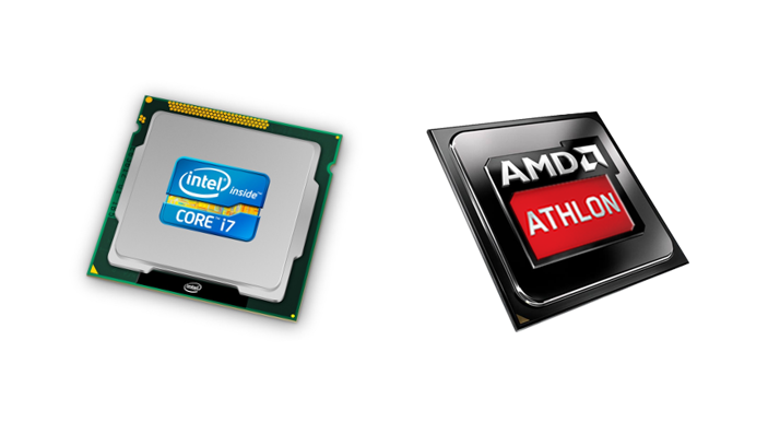
5. Intel, AMD
6. Socket - processor mounting method
7. How to choose a processor?
Technological process
The process of developing processors, if you get carried away, is an interesting activity. It all started with microcircuits, in which the frequency was measured in kilohertz. Then technologies improved, transistors became more and more, their sizes became smaller and smaller, thereby increasing the frequency, reducing power consumption and heat dissipation. As a result, today we have processors whose frequencies are measured in several gigahertz, and thanks to a decrease in the technical process, it is possible to fit several crystals (cores) in one substrate and place a huge number of transistors, plus add memory to the processor (cache).
As a result, we have efficient multi-core processors with high frequency, multi-level memory, reduced power consumption and relatively low heat dissipation.
Technological processes started from 10 micrometers (µm - 10 -6) and today's processes up to 10 nanometers (nm - 10 -9)
In short, the creation process: A piece of silicon is smelted into a cylindrical shape, then it is cut into thin plates and microcircuits are applied to them, then all this is mounted in a case and sealed. All stages of production are very complex and high-tech.
Here is what the plate looks like with microcircuits applied to it.
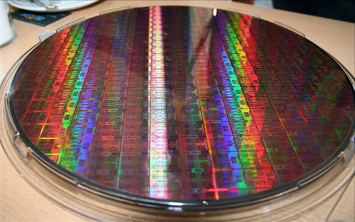
And a slightly enlarged version of the plate with ready-made crystals.

22nm and 20nm manufacturing processes correspond to the production of today's processors: Intel Ivy Bridge, Intel Haswell(Celeron, Pentium, Core i3, Core i5, Core i7).
Celeron and Pentium from this group in modern modifications. Slightly improved for affordability, added support for 64-bit capacity, cache - memory, but still poorly cope with modern tasks, especially Celeron.
The number of transistors in processors, since its inception, has varied from a couple of thousand to today's almost 2 billion!
I wonder if there is a limit?
CPU frequency
One could say that the higher the frequency, the better, but this is not at all the case. It is better if the processors are made according to the same architecture. In other cases, the performance depends on the processor architecture, the levels and size of the processor cache memory, as well as on the frequency system bus. If it is less (it is usually less), then the processor frequency will be reduced to its frequencies and the processor will be idle while data is transferred over the system bus (motherboard).
The first processor was introduced on November 15, 1971 and had a frequency of 740 kHz. Today, the most powerful processors can reach frequencies up to 5 GHz.
Another erroneous opinion exists (I myself heard from some) that if the processor is multi-core and its frequency is 2.6 GHz, then each core operates at this frequency. It's absolutely not true! This is the total frequency of all cores. This maximum frequency must be divided by the number of cores and you get the frequency of one core.
Below is an approximate graph of changes in processor frequency (GHz) and process technology (nm).
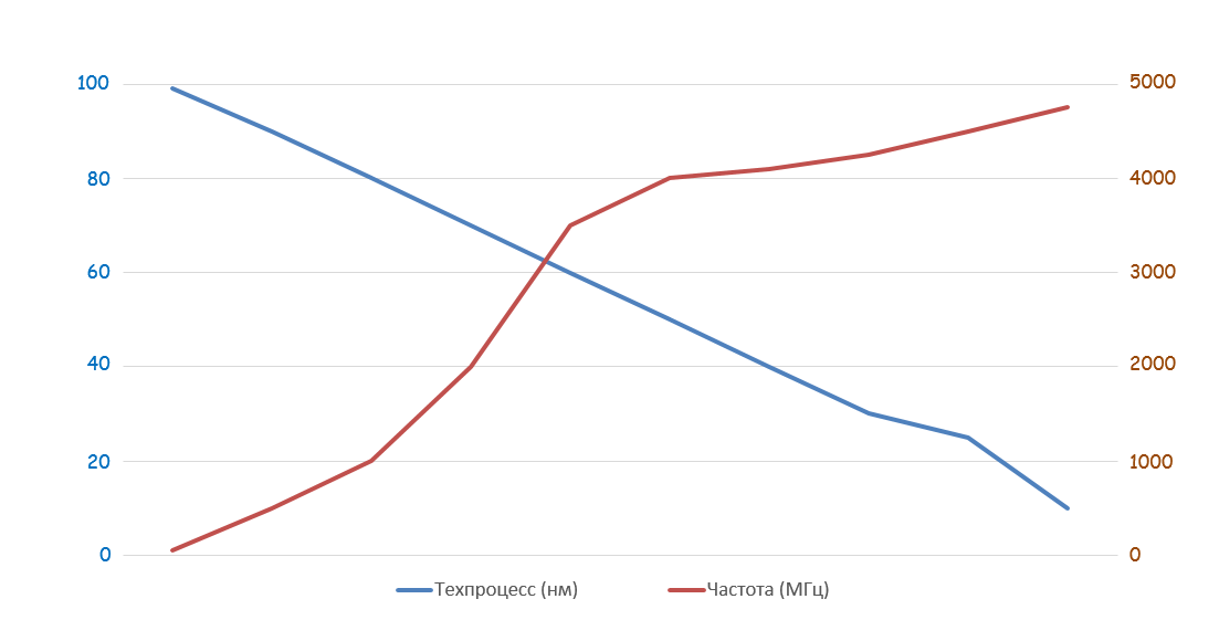
Over time, the process becomes smaller, and the frequency increases and power consumption decreases.
Heat dissipation (TDP)
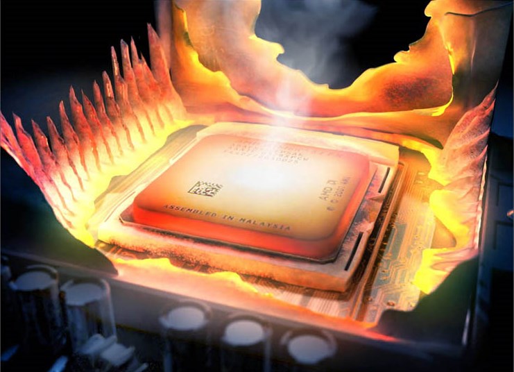
Processors allocate a large number of heat, without cooling, in just four seconds they can heat up to 90 degrees and naturally burn out, and if there is an overheating protection system, then turn off the system.
Therefore, it is important to monitor the condition of the radiator with the cooler, periodically clean it from dust, lubricate the cooler or replace it if necessary. Overheating can also be the result of braking and freezing of the system.
If we compare heat dissipation between processor manufacturers Intel and AMD, then the latter have much higher heat dissipation. Which in general does not suit me personally. Since the processor will heat up more, therefore, the cooling will work more intensively, pump more air and dust along with it, which leads to an early clogging of the radiator and cooler, an increase in dust crust, blockage of the radiator fins, obstruction of the passage of air and overheating, as well as noise from intensive rotation of the cooler, because it will try to cool the system with more power.
Cache - memory (SRAM), levels (L1, L2, L3)
Here I will describe the work in brief its work. You can read about all types of memory in the article Random Access Memory (RAM).
We have a processor, it has a memory of the first level L1, it operates at a frequency equal to the frequency of the processor, that is, the data stored in this memory will instantly go to the processor for processing. If this data is not in this memory, then the L2 level memory is accessed, which is slightly slower, but its volume is slightly larger. Further, if there is no data in the higher memory, the L3 level memory is accessed, if any, similarly it is slower, but larger. And lastly, there is an appeal to random access memory.
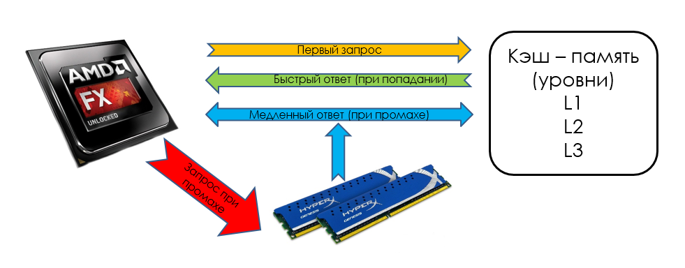
While the RAM is being accessed, the processor is idle. Downtime takes a little time, some fractions of a second, but in the aggregate it can take a long time.
Intel, AMD
It is Intel and AMD that are the market leaders in the production of processors, especially Intel with a share of about 87%.
I will not start with the most ancient processors, but let's go over the most popular today. The list is general, since other technical processes under their code names can also be included in the microarchitecture:
Nehalem(1st generation).
64-bit processors: EM64T - Microarchitecture Sandy Bridge(2nd generation)
64-bit processors: EM64T - Microarchitecture Ivy Bridge(3rd generation)
64-bit processors: EM64T - Microarchitecture Haswell(4th generation)
In the first and second Generation Intel Celeron and Intel Pentium should not even be considered when buying, they have already outlived their usefulness, modern tasks do not pull out.
i3, i5, i7 are separated by generation very simply, by the first digit in the marking, for example:
Intel Core i3 2100T - 2.5 GHz, the first digit in 2100T is 2, which means the second generation processor.
Intel Core i5 3450 - 3.1 GHz, the first digit in 3450 is 3, which means the third generation processor.
Intel Core i7 4770 - 3.4 GHz, the first digit in 4770 is 4, which means the third generation processor.
If the marking does not contain the first digits 2,3,4, then it is more likely a first-generation processor.
Let's take a look at AMD's current FX processor line.
AMD Desktop Microarchitecture - Bulldozer
Quad-core processors:
Six-core processors:
Octa-core processors:
The common difference between all of them is the support for some technologies that we do not need, the number of cores and the frequency of the processor. The main difference is the price. I still wrote that I dislike AMD for its huge heat dissipation, but you can choose a model comparable in power to Intel, but cheaper. Although if the processor gets hotter, you need suitable cooling, which will also cost a pretty penny, so maybe you shouldn’t look for an analogue at a cheaper price?
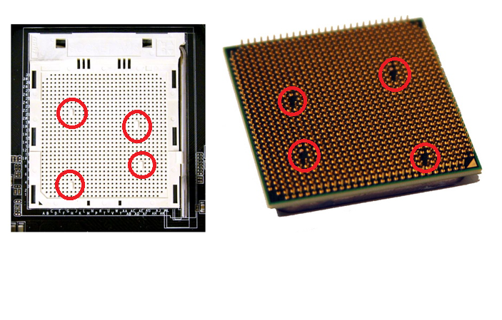
Socket - processor mounting method
Socket (Socket) - a special connector on the motherboard, designed to install the processor. On motherboards, manufacturers indicate which types of processors they support, you can read this on the box or in the description. And the description of the processors also indicates which sockets they support. So be careful. This also applies to the CPU heatsink mounts. Radiator mounts can be universal, that is, suitable for several sockets.
When installing the processor on the motherboard, there are "keys" (labels) for correct installation. For example, a beveled corner on the processor and socket, or protrusions or recesses in the processor substrate and vice versa on the socket.
An example of how labels look on Socket AM3
Socket 775 Example

And the last example of Sockets LGA 1366, 1150, 1155, 1156. They seem to look the same, but when you install the processor, you will see the difference and the impossibility of incorrect installation in the socket. You need to read the description or specifications.
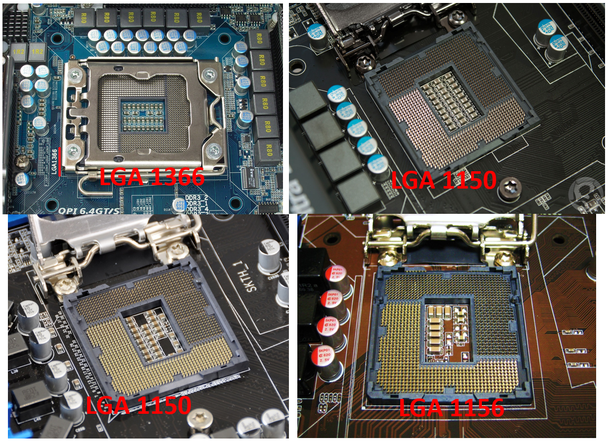
Why such diversity? The production of processors is constantly being improved, the number of pins is changing, and in order to avoid confusion in the support and installation of the processor, they come up with different ways mounts.
How to choose a processor?
If it's for games, then you still have to pay extra for integrated graphics, because top-end processors come with integrated video, plus fork out for a powerful video card. It all depends on your preferences. What will you use your computer for? If for working with documents, surfing the Internet, watching videos, then not the most powerful processor. I would also attribute that they did not choose with integrated graphics, but the trend is that almost all processors are already implementing it. Even probably for the better, you do not need to buy a video card separately.
Probably the most the best option today it would be the purchase of the second generation i5 processor from Intel, in the extreme case i3 on the LGA1155 socket, since these processors are in a more or less affordable price category. Processors on the i7 are too expensive and in the future, when prices drop, you can easily upgrade to a more powerful processor. In my opinion, the rest of the modifications should not be considered, they are on sockets of previous generations, without the possibility of updating the configuration.
For example, I still have motherboard on Socket LGA775 with an Intel Core 2Duo processor since 2008. The maximum way I can upgrade it is to add RAM and, for example, put SSD drive. If I want to improve my computer, I will have to update the entire computer, since my motherboard no longer supports new generation processors, only DDR2 RAM is supported, and in the new ones DDR3 or 4.
In any case, you should focus on processors that support the current and widespread Socket in order to be more likely to update your hardware configuration in the future. Although there is a possibility that new types of processors and connectors will appear, so buy what is currently on the market. There is also a rumor that Intel processors will only support operating system Windows 10 and above, who does not like it, is also worth considering.
There is such a wonderful site CPUBoss, where you can compare processors with each other in terms of performance, parameters and price. So drive in the name of the processors and choose the best one for you.
Transistor. Interesting facts
- The first portable radio had only four transistors, the first Intel microprocessor had 2,300 transistors, and the latest quad-core Intel processors based on 45nm manufacturing technology, launched on the market in November 2007, have up to 820 million transistors.
- The size of a 45nm transistor is 2,000 times smaller than the diameter of a human hair.
- Over 30 million 45nm transistors can fit on a pinhead.
- The first transistor, designed by the Bell Labs research center in 1947, could be handled, while hundreds of the latest 45-nm transistors from Intel can fit on the surface of a single human red blood cell.
- The cost of a transistor integrated on a chip latest processor Intel, about a million times lower than the average cost of a semiconductor transistor, which became the basis of integrated circuits in 1968. If car prices were falling as rapidly, a new car would cost about 1 cent today.
- Analysts estimate that the number of processors shipped annually on the planet is about 1019 transistors, which is about 100 times the entire population of ants living on Earth.
Stages of a long journey
Televisions, automobiles, radios, medical and household appliances, computers, space shuttles, and even programmable door locks in hotels - it's probably hard to imagine at least one more or less complex electronic device that surrounds us that would not use transistors. . The invention of the transistor 60 years ago at Bell Labs was a major driver of many remarkable innovations and advances in technology. In fact, without the transistor, the existence of almost the entire modern electronic-digital industry would be impossible. It was the transistor - a tiny device, a microcircuit element that acts like a miniature switch and thereby allows the implementation of information processing algorithms - that ensured the phenomenal triumph of computers.
What is the secret of success? Microelectronics is steadily developing, constantly enriching the scientific and technical community with innovations. Transistors with each new generation of technological processes for their manufacture are becoming more compact, faster, and more energy efficient. In November 2007, Intel engineers - for the first time in the long history of semiconductor integrated circuits - broke the silicon "monopoly" in the production of transistors and introduced new materials into the structure of semiconductor components. This enabled the creation of microprocessors based on the Intel® Core™ microarchitecture, using a revolutionary 45nm manufacturing technology using a high-k hafnium gate insulator (dielectric) and a metal gate, which provides record-breaking performance and efficient Energy consumption.
What's next? Intel is committed to continuing to push the boundaries of what's possible through technological innovation to create new products that can transform the way we work, play, and communicate in a meaningful way.
"On off"
The official date of the birth of the first transistor is December 23 (according to other sources - December 16), 1947, the authors of this wonderful invention were American physicists William Shockley, John Bardeen and Walter Brattain. True, initially the scientific community met this invention rather coolly, but already in 1956 all three Americans were awarded the Nobel Prize in Physics. Moreover, subsequently John Bardeen became the only Nobel laureate in the entire history of the Nobel Prize twice in the same nomination: the second prize in physics was awarded to him in 1972 for the creation of the theory of superconductivity.
Well, the name itself - “transistor” was invented by their colleague John R. Pierce. In May 1948, he won an internal competition organized among laboratory staff for the best name for an invention that was only a few months old at that time. The word "transistor" is formed by combining two terms: "transconductance" (active interelectrode conductivity) and "variable resistor" or "varistor" (variable resistance, varistor).
The first to actively use transistors were radio amateurs who used these elementary devices to amplify the signal. That is why the first portable wireless radios of the fifties were called transistorized, or even simply “transistors”. However, over time, they began to be used mainly as elements of integrated circuits, which provided the transistor with a crucial role in the technical achievements of mankind over the past forty years.
It's interesting to note that a transistor essentially does what a normal switch does: turns current on and off. The on position for the transistor means "1", the off position - "0". A huge number of transistors of an integrated circuit generates ones and zeros, which add up to a binary code understandable to a computer - a “language” that computers use in the process of calculations, word processing, movie and audio playback, display of images ...
Transistors and... rock'n'roll
The first transistor, in which current flowed along the surface of a semiconductor, was used to amplify the electrical signal passing through it - transistors coped with this task more efficiently than popular at that time, but more bulky and fragile electronic tubes.
In order to accelerate the popularization of transistors as much as possible, the Bell Labs research and development center decided to license transistor technology. A license worth $25,000 was purchased by twenty-six companies. However, for the commercial success of transistor technology, it was necessary to attract the attention of a mass audience. This was made possible by transistor radios. The first model of such a device, containing as many as four transistors, was introduced in October 1954. With the advent of a portable radio receiver, radio fans gained the opportunity to listen to music and receive information anywhere - this was immediately taken advantage of by young people who got the opportunity to escape from parental care and assert themselves with the help of a new subculture. So portable radio stimulated a new revolution ... and in music - rock and roll sounded everywhere on the air!
integrated circuit
By the end of the 50s, the transistor "settled" in radios, telephones and computers, and although its size was much smaller than that of vacuum tubes, this was clearly not enough to create a new generation of electronic devices. Another invention was needed to realize the huge computational potential of transistors, adapt them for mass production and reduce the cost.
In 1958, Jack Kilby of Texas Instruments and Robert Noyce of Fairchild Semiconductor, who later became one of the founding fathers of Intel Corporation, invented a way to combine a large number semiconductor transistors into a single integrated circuit, or microchip. This was a gigantic step forward - after all, previously individual components electrical circuit had to be connected manually.
Chips had two advantages: lower cost and higher performance. Both advantages were the result of miniaturization, which allowed for exponential reduction in the size of devices and extraordinary dynamism in the manufacturing process. Gordon Moore, who co-founded the processor giant Intel with Noyce in 1968, formulated a prediction published in 1965 called "Moore's law" in a journal article. According to this law, the number of transistors in a microcircuit should have doubled every one and a half to two years, which in turn would provide an increase in computing power and a decrease in the final cost of the product during its mass production. The ability to accommodate many compact elements on a small surface has proven to be a critical factor in the successful advancement of microcircuits.
Chip manufacturers have been able to sustain this exponential increase in transistor density per chip for decades. The first Intel® 4004 computer microprocessor, released in 1971, contained 2300 transistors. In 1989, the Intel® 486 processor had 1,200,000, and in 2000 the Intel® Pentium® 4 processor passed the 42 million milestone. The new 45nm quad-core Intel® Core™ 2 Extreme processor contains 820 million transistors.
Atom Games
Moore's Law is constantly predicted to die. Infinite exponential growth is impossible by definition - and yet processor manufacturers still manage to get around the limitation. In September last year, Gordon Moore said that the law named after him has every chance of remaining in force for at least another 10-15 years, but then new fundamental barriers to its implementation may arise. One way or another, but this most famous law of the computer world of the XXI century was in for hard times.
The battle for miniaturization has exhausted one of the most critical components of the transistor: the layer of silicon dioxide (SiO2) that acts as an insulating layer between the transistor's gate and its channel, which carries current when the transistor is on. With each new generation of processors, this insulating layer became thinner - until two generations ago its thickness reached 1.2 nm, or 5 atoms. Intel engineers were no longer able to make this layer even one more atom thinner.
As the thickness of the insulating layer decreases, the leakage current increases. The insulating layer began to pass current into the transistor, the behavior of the device changed, it began to dissipate more and more energy. As a result, the current consumption of the processor increased, and an additional amount of heat was released during its operation.
fundamental limit
Current leakage in the transistor became the most serious problem in the semiconductor industry: without a breakthrough in this area, the long-predicted fundamental limit became insurmountable. Moreover, this meant not only the end of Moore's law - the digital revolution of the last decades would suddenly stop. computer processors, which practically doubled its productivity every 24 months, could sink into oblivion.
To find a way out of the crisis, it was necessary to increase the thickness of the insulating layer, but to make this thicker layer from another dielectric material with a higher dielectric constant (high-k) to preserve the nature of the interaction between the gate and the channel. In January 2007, Intel announced that, for the first time in forty years, the insulating layer would not be silicon oxide, but a material based on hafnium, a silver-gray metal that has electrical properties superior to silicon and reduces leakage current by a factor of ten. Gordon Moore himself called this major achievement "the most important change in transistor technology since the late sixties."
However, this breakthrough solved the problem only half. The new material proved to be incompatible with an important component of the transistor - the gate. Even worse, transistors with the new insulating material performed less efficiently than those with the old one. Then it was proposed to replace the shutter material: Intel discovered a unique combination of metals, the composition of which is kept in strict confidence.
On November 12, 2007, Intel introduced a new generation of processors based on these materials and 45nm manufacturing technology. The new manufacturing technology, thinner than the previous 65nm, allowed Intel to nearly double the number of transistors in the same area of the chip - now it was possible to choose between increasing the total number of transistors or reducing the size of the processor. The new transistors require 30% less power to turn on and off. As a result, the new generation of Intel processors, manufactured using 45-nanometer manufacturing technology, not only demonstrates record performance, but also marks a breakthrough in power consumption.
The increase in computing power, which is a consequence of Moore's law, allows humanity to more effectively calculate ways to solve the most important problems facing it: climate change, hereditary diseases, the secrets of genetics, etc. It was difficult to even imagine modern ways and rates of solving such problems five years ago. New apps are helping to change our lives and make them even safer...
Number of transistors in the processor:
Processors and manufacturing technology: