There are two most popular processor architectures today. This is x86, which was developed back in the 80s and is used in personal computers and ARM is more modern, which allows you to make processors smaller and more economical. It is used in most mobile devices or tablets.
Both architectures have their pros and cons, as well as areas of application, but there are also common features. Many experts say that ARM is the future, but it still has some disadvantages that x86 does not have. In our today's article, we will look at how the arm architecture differs from x86. Consider the fundamental differences between ARM or x86, and also try to determine which is better.
What is architecture?
The processor is the main component of any computing device, be it a smartphone or a computer. Its performance determines how fast the device will work and how much it can run on battery. In simple terms, the processor architecture is a set of instructions that can be used in programming and implemented in hardware using certain combinations of processor transistors. They allow programs to interact with the hardware and determine how data will be transferred to and read from memory.
On the this moment There are two types of architectures: CISC (Complex Instruction Set Computing) and RISC (Reduced Instruction Set Computing). The first assumes that instructions for all occasions will be implemented in the processor, the second, RISC, sets the task for developers to create a processor with a set of commands that are minimally necessary for operation. RISC instructions are smaller and simpler.
x86 architecture
The x86 processor architecture was developed in 1978 and first appeared in Intel processors and belongs to the CISC type. Its name is taken from the model of the first processor with this architecture - Intel 8086. Over time, for lack of a better alternative, other processor manufacturers, such as AMD, began to support this architecture. It is now the standard for desktop computers, laptops, netbooks, servers and other similar devices. But sometimes x86 processors are also used in tablets, this is a fairly common practice.
The first Intel 8086 processor had a bit depth of 16 bits, then in 2000 a 32-bit architecture processor was released, and even later a 64-bit architecture appeared. We discussed in detail in a separate article. During this time, the architecture has developed very much, new instruction sets and extensions have been added, which can greatly increase the performance of the processor.
x86 has several significant drawbacks. Firstly, this is the complexity of the teams, their confusion, which arose due to a long history of development. Secondly, such processors consume too much power and generate a lot of heat because of this. The x86 engineers initially took the path of getting maximum performance, and speed requires resources. Before looking at the differences between arm x86, let's talk about the ARM architecture.
ARM architecture
This architecture was introduced a little later for x86 - in 1985. It was developed by Acorn, a well-known company in Britain, then this architecture was called Arcon Risk Machine and belonged to the RISC type, but then its improved version, Advanced RISC Machine, was released, which is now known as ARM.
When developing this architecture, the engineers set themselves the goal of eliminating all the shortcomings of x86 and creating a completely new and most efficient architecture. ARM chips received minimal power consumption and a low price, but had poor performance compared to x86, so they initially did not gain much popularity on personal computers.
Unlike x86, developers initially tried to get minimum costs on resources, they have fewer processor instructions, fewer transistors, but, accordingly, fewer any additional features. But in recent years, the performance of ARM processors has improved. Given this, and low power consumption, they began to be very widely used in mobile devices such as tablets and smartphones.
Differences between ARM and x86
And now that we have looked at the history of the development of these architectures and their fundamental differences, let's make a detailed comparison of ARM and x86, according to their various characteristics, in order to determine which is better and more accurately understand what their difference is.
Production
x86 vs arm production is different. x86 processors are produced only by two companies, Intel and AMD. Initially, this was one company, but this is a completely different story. Only these companies have the right to release such processors, which means that only they will manage the direction of infrastructure development.
ARM works very differently. The company that develops ARM doesn't release anything. They simply issue permission to develop processors of this architecture, and already manufacturers can do whatever they need, for example, release specific chips with the modules they need.
Number of instructions
These are the main differences between the arm and x86 architectures. x86 processors have evolved rapidly as more powerful and productive. The developers have added a large number of processor instructions, and here there is not just a basic set, but a lot of commands that could be dispensed with. Initially, this was done to reduce the amount of memory occupied by programs on disk. Also, many protection and virtualization options, optimizations and much more have been developed. All this requires additional transistors and energy.
ARM is more simple. There are much fewer processor instructions here, only those that are needed by the operating system and are actually used. If we compare x86, then only 30% of all possible instructions are used there. They are easier to learn if you decide to write programs by hand, and they require fewer transistors to implement.
Power consumption
Another conclusion emerges from the previous paragraph. The more transistors on the board, the greater its area and power consumption, and vice versa.
x86 processors consume much more power than ARM. But power consumption is also affected by the size of the transistor itself. For example, an Intel i7 processor consumes 47 watts, and any ARM processor for smartphones consumes no more than 3 watts. Previously, boards with a single element size of 80 nm were produced, then Intel achieved a reduction to 22 nm, and this year scientists were able to create a board with a element size of 1 nanometer. This will greatly reduce power consumption without sacrificing performance.
In recent years, the power consumption of x86 processors has been greatly reduced, for example, new processors Intel Haswell can last longer on battery power. Now the difference arm vs x86 is gradually being erased.
Heat dissipation
The number of transistors affects another parameter - this is heat generation. Modern devices cannot convert all the energy into effective action, some of it is dissipated as heat. The efficiency of the boards is the same, which means that the fewer transistors and the smaller their size, the less heat the processor will generate. There is no longer a question of ARM or x86 will generate less heat.
Processor performance
ARM wasn't built for maximum performance, that's where x86 thrives. This is partly due to the smaller number of transistors. But recently, the performance of ARM processors has been growing, and they can already be fully used in laptops or on servers.
findings
In this article, we looked at how ARM differs from x86. The differences are quite serious. But lately, the line between both architectures has been blurred. ARM processors are becoming more productive and faster, and x86, due to the reduction in the size of the structural element of the board, begin to consume less power and generate less heat. You can already find ARM processors on servers and laptops, and x86 processors on tablets and smartphones.
And how do you feel about these x86 and ARM? What technology is the future in your opinion? Write in the comments! By the way, .
At the end of the video about the development of ARM architecture:
Main features of architecture
SSE4 consists of 54 instructions, 47 of them belong to SSE4.1 (they are only in Penryn processors). The full instruction set (SSE4.1 and SSE4.2, i.e. 47 + remaining 7 instructions) is available in Nehalem processors. None of the SSE4 instructions work with 64-bit mmx registers, only with 128-bit xmm0-15. 32-bit processors with SSE4 were not released.
Instructions have been added to speed up motion compensation in video codecs, fast reading from USWC memory, a lot of instructions to simplify the vectorization of programs by compilers. In addition, instructions for processing strings of 8/16 bit characters, CRC32 calculations, popcnt have been added to SSE4.2. For the first time in SSE4, the xmm0 register was used as an implicit argument for some instructions.
New SSE4.1 instructions include video acceleration, vector primitives, insertion/extraction, vector dot multiplication, blending, bit checking, rounding, and reading WC memory.
New SSE4.2 instructions include string processing, CRC32 counting, counting a population of 1 bits, and working with vector primitives.
SSE5
AMD's new x86 instruction extension called SSE5. This brand new SSE instruction set, created by AMD, will be supported by up-and-coming CPU companies starting in 2009.
SSE5 brings to the classic x86 architecture some of the features that were previously available exclusively in RISC processors. The SSE5 instruction set defines 47 new basic instructions designed to speed up single-threaded computations by increasing the "density" of processed data.
There are two main groups of new instructions. The first includes instructions that accumulate the results of multiplication. Instructions of this type can be useful for organizing iterative computational processes when rendering images or when creating three-dimensional audio effects. The second group of new instructions includes instructions that operate on two registers and store the result in a third. This innovation may allow developers to do without unnecessary transfers of data between registers in computational algorithms. SSE5 also contains several new instructions for comparing vectors, for permuting and moving data, and for changing precision and rounding.
The main applications for SSE5 AMD sees computational tasks, multimedia content processing and encryption tools. It is expected that in computing applications using matrix operations, the use of SSE5 can give a 30% performance increase. Multimedia tasks that require a discrete cosine transform can get a 20% speedup. And encryption algorithms thanks to SSE5 can get a fivefold gain in data processing speed.
AVX
The next set of extensions from Intel. The processing of floating-point numbers packed into 256-bit "words" is supported. For them, support for the same commands is introduced as in the SSE family. 128-bit SSE registers XMM0 - XMM15 expand to 256-bit YMM0-YMM15
Intel Post 32nm processor extensions - a new Intel instruction set that allows you to convert half-precision numbers to single and double precision numbers, get true random numbers in hardware and access FS / GS registers.
AVX2
Further development of AVX. SSE integer instructions start working with 256-bit AVX registers.
AES
AES command set extension - microprocessor implementation of AES encryption.
3DNow!
A set of instructions for stream processing single-precision real numbers. Supported by AMD processors since K6-2. Not supported by Intel processors.
3DNow! use MMX registers as operands (two single precision numbers are placed in one register), therefore, unlike SSE, when switching tasks, it is not necessary to save the 3DNow! context separately.
64-bit mode
Superscalar means that the processor can perform more than one operation per clock cycle. Super-pipelining means that the processor has multiple computation pipelines. The Pentium has two of them, which allows it to ideally be twice as productive as the 486 at the same frequencies, executing 2 instructions per clock at once.
In addition, the Pentium processor featured a completely redesigned and very powerful FPU at that time, the performance of which remained unattainable for competitors until the late 1990s.
Pentium Over Drive
In addition, an MMX block was added to the Pentium II core.
Celeron
The first representative of this family was based on the Pentium II architecture, it was a cartridge with a printed circuit board on which the core, L2 cache and cache tag were mounted. Mounted in slot Slot 2.
Modern Xeons are based on the Core 2 / Core i7 architecture.
AMD Processors
Am8086 / Am8088 / Am186 / Am286 / Am386 / Am486Fundamentally new AMD processor(April 1997), based on a kernel purchased from NexGen. This processor had a fifth-generation construct, but belonged to the sixth generation and was positioned as a competitor to the Pentium II. Included an MMX block and a somewhat redesigned FPU block. However, these blocks still worked 15-20% slower than those of similar frequency Intel processors. The processor had 64 KB of L1 cache.
Overall, Pentium II-like performance, compatibility with older motherboards, and an earlier launch (AMD introduced the K6 a month earlier than Intel introduced the P-II) and lower price made it quite popular, but AMD's production problems significantly spoiled the reputation of this processor.
K6-2Further development of the K6 core. These processors have added support for the specialized 3DNow! . The real performance, however, turned out to be significantly lower than that of similarly clocked Pentium IIs (this was due to the fact that the performance increase with increasing frequency was higher for the P-II due to the internal cache) and only the Celeron could compete with the K6-2. The processor had 64 KB of L1 cache.
K6-IIIMore technologically successful than the K6-2, an attempt to create an analogue of the Pentium III. However, it was not a marketing success. It is distinguished by the presence of 64 KB of the first level cache and 256 KB of the second level cache in the core, which allowed it to outperform the Intel Celeron in terms of performance at an equal clock frequency and not be significantly inferior to the early Pentium III.
K6-III+Similar to K6-III with PowerNow! and more high frequency and an extended set of instructions. Originally intended for laptops. It was also installed in desktop systems with a Super 7 processor socket. Used to upgrade desktop systems with a Socket 7 processor socket (Only on motherboards that supply two voltages to the processor, the first for processor I / O blocks and the second for the processor core. Not all manufacturers provided dual power on the first models of their motherboards with a socket socket 7).
An analogue of K6-III + with a cache of the second level cut down to 128 KB.
AthlonA very successful processor, thanks to which AMD was able to regain its almost lost position in the microprocessor market. First level cache - 128 KB. Initially, the processor was produced in a cartridge with a second-level cache (512 KB) on the board and installed in Slot A (which is mechanically, but not electrically compatible with Intel's Slot 1). Then I switched to Socket A and had 256 KB of L2 cache in the core. In terms of speed - an approximate analogue of the Pentium III.
DuronA stripped-down version of Athlon differs from its parent in the size of the L2 cache (only 64 KB, but integrated into the chip and running at the core frequency).
Celeron competitor of the Pentium III / Pentium 4 generations. The performance is noticeably higher than that of similar Celerons, and it matches the Pentium III in many tasks.
Athlon XPContinued development of the Athlon architecture. In terms of performance, it is analogous to the Pentium 4. Compared to regular Athlon, support for SSE instructions has been added.
SempronA cheaper (due to the reduced L2 cache) version of the Athlon XP and Athlon 64 processors.
The first Sempron models were relabeled Athlon XP chips based on Thoroughbred and Thorton cores, which had 256 KB of L2 cache and worked on a 166 (333 DDR) bus. Later, stripped-down versions of Athlon 64/Athlon II were produced (and are being produced) under the Sempron brand, positioned as competitors to Intel Celeron. All Semprons have a truncated level 2 cache; younger Socket 754 models had Cool&quiet and x86-64 blocked; Socket 939 models had a blocked dual-channel memory mode.
OpteronFirst processor to support the x86-64 architecture.
Athlon 64The first non-server processor to support the x86-64 architecture.
Athlon 64X2Continuation of the Athlon 64 architecture, has 2 cores.
Athlon FX
had a reputation for being "the fast processor for toys. Is, in fact, server processor Opteron 1xx on desktop sockets without registered-memory support. Produced in small batches. It costs much more than its "mass" counterparts.
PhenomA further development of the Athlon 64 architecture, it is available in versions with two (Athlon 64 X2 Kuma), three (Phenom X3 Toliman) and four (Phenom X4 Agena) cores.
Phenom IIVIA processors
Cyrix III / VIA C3First processor released under the VIA brand. Released with different kernels from different development teams. Socket 370 connector.
The first release is based on the Joshua kernel, acquired by VIA along with the Cyrix development team.
The second release is with the Samuel kernel, developed on the basis of the never-released IDT WinChip -3. It was distinguished by the absence of a cache memory of the second level and, accordingly, an extremely low level of performance.
The third release is with the Samuel-2 kernel, an improved version of the previous kernel, equipped with a second-level cache. The processor was produced using thinner technology and had reduced power consumption. After the release of this core, the VIA Cyrix III brand finally gave way to VIA C3.
The fourth release is with the Ezra core. There was also an Ezra-T variant adapted to work with a bus designed for Tualatin core Intel processors. Further development in the direction of energy saving.
The fifth release is with the Nehemiah kernel (C5P). This core finally got a full speed coprocessor, support for instructions or .
Processors based on the V33 core did not have an 8080 emulation mode, but they supported it, using two additional instructions, extended addressing mode.
NexGen processors
Nx586In March 1994, the NexGen Nx586 processor was introduced. It was positioned as a Pentium competitor, but initially did not have an integrated coprocessor. The use of a proprietary bus entailed the need to use proprietary chipsets, NxVL (VESA Local Bus) and NxPCI 820C500 (PCI), and an incompatible processor socket. The chipsets were developed jointly with VLSI and Fujitsu. The Nx586 was a superscalar processor and could execute two instructions per clock. The L1 cache was separate (16 KB for instructions + 16 KB for data). The L2 cache controller was integrated into the processor, while the cache itself was located on motherboard. Just like the Pentium Pro, the Nx586 was a RISC processor inside. The lack of support for CPUID instructions in early modifications of this processor led to the fact that it was defined programmatically as a fast 386 processor. It was also connected with the fact that Windows 95 refused to be installed on computers with such processors. To solve this problem, a special utility (IDON.COM) was used, which represented the Nx586 for Windows as a 586 class CPU. Nx586 was produced at the facilities of IBM.
An Nx587 FPU co-processor was also developed, which was mounted at the factory on top of the processor die. Such "assemblies" were labeled Nx586Pf. When designating the performance of Nx586, P-rating was used - from PR75 (70 MHz) to PR120 (111 MHz).
The next generation of NexGen processors, which was never released, but served as the basis for the AMD K6.
SiS processors
SiS550The SiS550 SoC family is based on the licensed Rise mP6 core and is available at frequencies from 166 to 266 MHz. At the same time, the fastest solutions consume only 1.8 watts. The kernel has three integer 8-stage pipelines. Cache L1 separate, 8+8 KB. The built-in coprocessor is pipelined. The SiS550, in addition to the standard set of ports, includes a 128-bit AGP 4x UMA video core, 5.1-channel audio, support for 2-instructions called Code Morphing Software. This allows the processor to adapt to any set of instructions and improves energy efficiency, but the performance of such a solution is obviously less than that of processors with a native x86 instruction system. math coprocessor, and variants with a coprocessor were supposed to be called U5D, but were never released.
Intel obtained an injunction against the sale of Green CPUs in the US, arguing that UMC used Intel microcode in its processors without a license.
There were also some problems with the software. For example, the game Doom refused to run on this processor without changing the configuration, and Windows 95 would freeze from time to time. This was due to the fact that programs found a missing coprocessor in the U5S and attempts to access it ended in failure.
Processors produced in the USSR and Russia
KR1810VM86BLX IC Design/ICT Processors
BLX IC Design and Institute computer technology China has been developing MIPS-based processors with hardware translation of x86 instructions since 2001. These processors are produced by STMicroelectronics. A partnership with TSMC is being considered.
Godson (Longxin, Loongson, Dragon)
Godson is a 32-bit MIPS-based RISC processor. Technology - 180 nm. Introduced in 2002. Frequency - 266 MHz, a year later - a version with a frequency of 500 MHz.
Godson 2
- Godson 2 is a 64-bit RISC processor based on MIPS III. 90 nm technology. At an equal frequency, it outperforms its predecessor by 10 times in performance. Introduced April 19, 2005.
- Godson-2E - 500 MHz, 750 MHz, later - 1 GHz. Technology - 90 nm. 47 million transistors, power consumption - 5 ... 7.5 W. The first Godson with hardware translation of x86 commands, and up to 60% of processor performance is spent on it. Introduced in November 2006.
- Godson 2F - 1.2 GHz, available since March 2007. An increase in performance compared to its predecessor by 20-30% is declared.
- Godson 2H - scheduled for release in 2011. It will be equipped with an integrated video core and memory controller and is intended for consumer systems.
- Godson 3 - 4 cores, 65nm technology. Power consumption - about 20 watts.
- Godson 3B - 8 cores, 65 nm technology (28 nm is planned), clock frequency within 1 GHz. Crystal area - 300 mm². Floating point performance is 128 GigaFLOPS. Power consumption of 8-core Godson 3-40W. Translation to x86 code is performed using a set of 200 instructions, and translation consumes about 20% of the processor's performance. The processor has a 256-bit vector SIMD processing unit. The processor is intended for use in servers and embedded systems.
The structure of an arbitrary instruction is as follows:
- Prefixes (each one is optional):
- One-byte address change prefix AddressSize (value 67h).
- One-byte Segment change prefix (values 26h, 2Eh, 36h, 3Eh, 64h, and 65h).
- A one-byte BranchHint prefix to indicate the preferred branch of the branch (values 2Eh and 3Eh).
- A 2-byte or 3-byte complex Vex prefix (the first byte is always C4h for the 2-byte version or C5h for the 3-byte version).
- One-byte Lock prefix to prevent memory modification by other processors or cores (value F0h).
- One-byte prefix OperandsSize to change the size of the operand (value 66h).
- One-byte Mandatory prefix for instruction qualification (values F2h and F3h).
- The single-byte prefix Repeat means repetition (values F2h and F3h).
- The one-byte Rex structured prefix is needed to specify 64-bit or extended registers (values 40h..4Fh).
- Escape prefix. Always consists of at least one 0Fh byte. This byte is optionally followed by byte 38h or 3Ah. Designed to clarify instructions.
- Instruction-specific bytes:
- Byte Opcode (arbitrary constant value).
- Byte Opcode2 (arbitrary constant value).
- Byte Params (has a complex structure).
- Byte ModRm is used for operands in memory (has a complex structure).
- The SIB byte is also used for operands in memory and has a complex structure.
- Data embedded in the instruction (optional):
- Offset or address in memory (Displacement). A signed integer of size 8, 16, 32, or 64 bits.
- The first or only immediate operand (Immediate). Can be 8, 16, 32 or 64 bits.
- Second immediate operand (Immediate2). If present, it is usually 8 bits in size.
In the list above and below, for technical names, the name “only Latin, Arabic numerals” and the minus sign “-” with an underscore “_” are accepted, and the case is CamelCase (any word starts with an uppercase, and then only lowercase, even if the abbreviation is: “ UTF-8" → "Utf8" - all words together). The AddressSize, Segment, BranchHint, Lock, OperandsSize, and Repeat prefixes can be intermixed. The rest of the elements must go exactly in the specified order. And you can see that the byte values of some prefixes are the same. Their purpose and presence is determined by the instruction itself. Segment override prefixes can be used with most instructions, while BranchHint prefixes can only be used with conditional branch instructions. The situation is similar with the Mandatory and Repeat prefixes - somewhere they specify the instruction, and somewhere they indicate repetition. The OperandSize prefix together with the Mandatory prefixes are also referred to as SIMD instruction prefixes. Separately, it should be said about the Vex prefix. It replaces the Rex, Mandatory, Escape and OperandsSize prefixes, compacting them into itself. It is not allowed to use the Lock prefix with it. The Lock prefix itself can be added when the destination is an operand in memory.
An overview list of all modes of interest in terms of instruction coding:
- 16-bit ("Real Mode", real mode with segment addressing).
- 32-bit ("Protected Mode", a protected mode with a flat memory model).
- 64-bit ("Long Mode", as 32-bit protected with a flat memory model, but the addresses are already 64-bit).
In parentheses, the English names of the modes correspond to the official ones. There are also synthetic modes like Unreal x86 Mode, but they all follow from these three (in fact, they are hybrids that differ only in address size, operands, etc.). Each of them uses the "native" addressing mode, but it can be changed to an alternative one with the OperandsSize prefix. In 16-bit mode, 32-bit addressing will be enabled, in 32-bit mode, 16-bit addressing, and in 64-bit mode, 32-bit addressing. But if this is done, then the address is zero-padded (if it is less) or its high-order bits are reset (if it is greater).
4.6. Features of the architecture of modern x86 processors
4.6.1. Processor architecture Intel Pentium(P5/P6)
Pentium family processors have a number of architectural and structural features compared to previous models of Intel microprocessors. The most typical of them are:
Harvard architecture with separation of command and data streams by introducing separate internal cache memory blocks for storing commands and data, as well as buses for their transmission;
Superscalar architecture that provides simultaneous execution of several commands in parallel operating devices;
Dynamic command execution, which implements a change in the sequence of commands, the use of an extended register file (register renaming) and efficient branch prediction;
Dual independent bus containing a separate bus for accessing the L2 cache (runs at the processor clock speed) and a system bus for accessing memory and external devices(performed at the motherboard clock rate).
The main characteristics of the Pentium family of processors are as follows:
32-bit internal structure;
Using a system bus with 36 address bits and 64 data bits;
Separate internal cache memory of the first level for instructions and data with a capacity of 16 KB;
Support for a shared cache memory of commands and data of the second level with a capacity of up to 2 MB;
Pipeline execution of commands;
Predicting the direction of software branching with high accuracy;
Accelerated execution of floating point operations;
Priority control when accessing memory;
Support for the implementation of multiprocessor systems;
Availability of internal tools that provide self-testing, debugging and performance monitoring.
New microarchitecture Pentium processors (rice. 4.6)and later is based on the method superscalar processing .
Under superscalar implied more one a pipeline for processing commands (as opposed to a scalar - single-pipeline architecture).
Figure 4.6 - Block diagram of the Pentium MP architecture
In the Pentium MP, commands are distributed over two independent execution pipelines (U and V). Conveyor U can execute any instruction of the IA-32 family, including integer and floating point instructions. Conveyor V designed to execute simple integer instructions and some floating point instructions. Commands can be sent to each of these devices simultaneously, and when a control device issues a pair of commands in one cycle, a more complex command enters the U pipeline, and a less complex one enters the V pipeline.
However, such pairwise processing of instructions (pairing) is only possible for a limited subset of integer instructions. Real arithmetic instructions cannot be paired with integer instructions. Simultaneous issuance of two commands is possible only if there are no register dependencies.
One of the main features of the sixth generation of microprocessors of the IA-32 architecture is dynamic(speculative) performance. This term refers to the following set of possibilities:
- deep branch prediction(with a probability > 90% it is possible to predict 10-15 nearest transitions);
- data flow analysis(view the program 20-30 steps ahead and determine the dependence of commands on data or resources);
- forward execution of commands(MP P6 may execute commands in an order different from their sequence in the program).
Internal organization of MP P6 conforms to the RISC architecture, so instruction fetch block, reading the IA-32 instruction stream from L1 instruction cache, decodes them into a series of micro-ops. The flow of micro-operations falls into reorder buffer (instruction pool). It contains micro-operations that have not yet been executed, as well as micro-operations that have already been executed, but have not yet affected the state of the processor.
To decode instructions, three parallel decoder: two for simple and one for complex instructions.
Each IA-32 instruction is decoded in 1-4 micro-ops. Micro-operations are performed five parallel actuators: two for integer arithmetic, two for real arithmetic and memory interface block. Thus, it is possible to perform up to five micro-ops per cycle.
Block of executive devices is able to select instructions from the pool in any order. At the same time, thanks to branch prediction block execution of instructions following conditional jumps is possible. Reservation unit constantly monitors in the instruction pool those micro-operations that are ready for execution (the initial data does not depend on the result of other unexecuted instructions) and directs them to a free execution unit of the appropriate type. One of the integer actuators is additionally involved in checking the correctness of branch prediction. When an incorrectly predicted transition is detected, all micro-operations following the transition are removed from the pool and the instruction pipeline is filled with instructions at the new address.
The interdependence of instructions on the value of the IA-32 architecture registers may require waiting for the registers to be released. To solve this problem, 40 general purpose internal registers used in real computing.
Delete block tracks the result of speculatively executed micro-ops. If a micro-op no longer depends on other micro-ops, its result is transferred to the processor state and it is removed from the reorder buffer. The delete block acknowledges the execution of instructions (up to three micro-ops per cycle) in the order in which they appear in the program, taking into account interrupts, exceptions, breakpoints, and branch prediction misses.
The described scheme is shown in fig. 4.7.

Figure 4.7 - Block diagram of the Pentium Pro microprocessor
4.6.2. SIMD extensions MMX
Many algorithms for working with multimedia data allow the simplest elements of parallelization, when one operation can be performed in parallel on several numbers. This approach is called SIMD - single-instruction multiple-data (one instruction - a lot of data). This technology was first implemented in the P55 generation (Pentium MMX microprocessor).
MMX (Multi-Media eXtension) is a SIMD extension for streaming integer data, implemented on the basis of the FPU (using FPU registers).
A single MMX instruction can perform an arithmetic or boolean operation on "packages" of integers packed in MMX registers. For example, the PADDSB instruction adds 8 bytes of one "package" to the corresponding 8 bytes of another package, effectively performing the addition of eight pairs of numbers in one instruction.
4.6.3. Processors Pentium Pro, Pentium II, Pentium III
The Pentium II processor combines the best properties of Intel processors: the performance of the Pentium Pro processor and the capabilities of MMX technology. This combination provides a significant performance increase for Pentium II processors over previous IA-32 architecture processors.
The processor contains separate internal instruction and data cache blocks of 16 KB and 512 KB of a common non-blocking L2 cache.
The performance improvement of IA-32 was achieved not only by optimizing the instruction pipeline and adding execution units, but also, for example, by introducing cache memory into the processor core. In the IA-32 family, an on-chip L1 cache of 8 KB was first implemented in the Intel-486 processors. In Pentium processors, the cache size has been doubled. The first representatives of the P6 (Pentium Pro) also contained an L2 cache of 256 or 512 KB. However, such a solution at that time turned out to be too expensive and unprofitable, so the Pentium II introduced the technology Dual Independent Bus (DIB) - double independent bus. Separate buses were used to access the cache and to access external memory. The same architectural solution was used in the first Pentium III models. Since 1999 (Pentium III Coppermine), the L2 cache has been returned to the inside of processor chips.
The development of the SIMD idea for real numbers was the technology SSE (Streamed SIMD Extensions), first introduced with Pentium III processors. The SSE block complements the MMX technology with eight 128-bit XMM0-XMM7 registers and a 32-bit MXCSR control and status register.
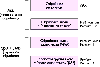
Figure 4.9 - Evolution of the data processing process in Intel Pentium processors
4.6.4. Pentium 4 (P7) - Net Burst microarchitecture
The Pentium 4 processor is a 32-bit representative of the IA-32 family, belonging to the new, seventh (according to Intel classification) generation microarchitecture. From a software point of view, it is an IA-32 processor with another extension of the command system - SSE2. In terms of the set of software-accessible registers, the Pentium 4 repeats the Pentium III processor. From an external, hardware point of view, this is a processor with a new type of system bus, in which, in addition to increasing the clock frequency, the already familiar principles of double (2x) and quadruple (4x) synchronization are applied, and a number of measures are taken to ensure performance at previously unthinkable frequencies. The microarchitecture of the processor, called Net Burst, is designed to take into account the high frequencies of both the core (more than 1.4 GHz) and the system bus (400 MHz).
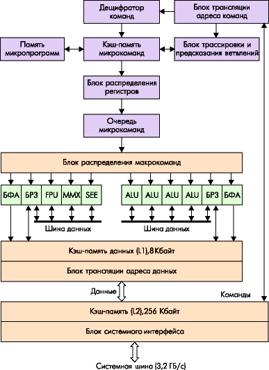
Figure 4.10 - NetBurst microarchitecture
The Pentium 4 processor is single-chip. In addition to the actual computing core, it contains a cache memory of two levels. The secondary cache, shared between instructions and data, has a size of 256 KB and a bus width of 256 bits (32 bytes), as in latest processors Pentium III. The secondary cache bus operates at the core frequency, which provides its bandwidth of 32x1.4 = 44.8 GB / s at a frequency of 1.4 GHz. The secondary cache has ECC control to detect and correct errors. The primary data cache has the same high bandwidth (44.8 GB / s), but its size has been halved (8 KB versus 16 in the Pentium III). There is no primary instruction cache in the usual sense, it has been replaced by the trace cache. It stores sequences of micro-ops into which instructions are decoded. Up to 12K microinstructions can fit here.
The processor system bus interface is designed for single processor configurations only. The interface is in many ways similar to the P6 bus, the protocol is also focused on the simultaneous execution of several transactions. A number of measures have been taken to ensure high throughput. In the Pentium 4 processor, the bus frequency is 400 MHz with "quad pumped" (quad pumped) - the system bus clock is 100 MHz, but the address and data transfer rate is higher. New information can be transmitted on the common timing lines every 100 MHz clock. For 2x and 4x transmission, synchronization from the data source is used.
MP actuators (ALUs) operate at double the frequency, which makes it possible to execute most integer instructions in half a cycle. Compared to previous generations of the IA-32, the Pentium 4 contains the longest instruction pipeline of 20 stages called hyperconveyor. In connection with this feature, many experts note that the NetBurst microarchitecture will have maximum performance execution of predictable (linear and cyclic) sections of the program, typical for applications that Pentium 4 is oriented towards. frequencies of 1.4 GHz and above. To partially compensate for this shortcoming, the mechanisms of speculative execution and branch prediction were significantly optimized.
The material of Chapter 4 is based on a generalization of works.
Disclaimer
Probably, the most accurate reason for the appearance of this material can be formulated as follows: "it is not even so much necessary that it be - it is rather strange that it has not yet been." And indeed: in the comments on the test results, we constantly operate with such concepts as “cache capacity”, “processor bus speed”, “support for extended instruction sets”, but there is no single article on the site that would contain explanations of all these terms. . Such an omission, of course, should be eliminated. This article, subtitled "x86 CPU FAQ", is an attempt to do just that. Of course, some of its sections can be attributed not only to x86 processors, and not only to their desktop (intended for installation in a PC) variants, but we definitely do not aim at such globalism. Therefore, please remember that for the purposes of this material, unless explicitly stated otherwise, the word "processor" means "an x86 processor intended for installation in desktops." Perhaps, in the process of further improvement and expansion, sections on server CPUs or even processors of other architectures will appear in the article, but this is a matter for the future ...
Introduction
Code and data: the basic principle of the processor
So, if you don’t try to present here a “briefly” computer science course for high school, then the only thing I would like to remind you is that the processor (with rare exceptions) does not execute programs written in any programming language (one of which, you , perhaps even know), but some "machine code". That is, the commands for it are sequences of bytes located in the computer's memory. Sometimes a command can be one byte, sometimes it takes several bytes. In the same place, in the main memory (RAM, RAM) there are also data. They can be in a separate area, or they can be "mixed" with the code. The difference between code and data is that data is what above what the processor performs some operations. And the code is the commands that tell it, which operation he must produce. To simplify, we can imagine a program and its data as a sequence of bytes of some finite length, located continuously (let's not complicate) in a common memory array. For example, we have a memory array with a length of 1'000'000 bytes, and our program (together with data) is bytes with numbers from 1000 to 20'000. Other bytes are other programs or their data, or just free memory not occupied by anything useful.
Thus, "machine code" is the instructions of the processor, located in memory. The data is located there. In order to execute an instruction, the processor must read it from memory. In order to perform an operation on data, the processor must read them from memory, and, possibly, after performing a certain action on them, write them back to memory in an updated (modified) form. Commands and data are identified by their address, which is essentially the ordinal number of a memory location.
General principles of interaction
processor and RAM
Perhaps it will surprise someone that a rather large section in the x86 CPU FAQ is dedicated to explaining the features of memory functioning in modern systems based on this type of processor. However, the facts are a stubborn thing: x86 processors themselves now contain so many blocks responsible specifically for optimizing their work with RAM that it would be completely ridiculous to ignore this close connection. You can even say this: since solutions related to optimizing memory work have become an integral part of the processors themselves, then the memory itself can be considered as a kind of “appendage”, the functioning of which has a direct impact on the speed of the CPU. Without understanding the peculiarities of the interaction of the processor with memory, it is impossible to understand due to what this or that processor (this or that system) executes programs slower or faster.
Memory controller
So, earlier above, we already said that both commands and data enter the processor from random access memory. In fact, everything is a little more complicated. In most modern x86 systems (that is, computers based on x86 processors), the processor, as a device, cannot access memory at all, since it does not include the corresponding nodes. Therefore, it refers to an "intermediate" specialized device called a memory controller, and that, in turn, to RAM chips located on memory modules. You must have seen the modules - these are such long narrow textolite "slats" (in fact, small boards) with a certain number of microcircuits on them, inserted into special connectors on the motherboard. The role of the RAM controller is therefore simple: it serves as a kind of "bridge" * between the memory and the devices using it (by the way, this includes not only the processor, but more on that later). As a rule, the memory controller is part of the chipset - a chipset that is the basis of the motherboard. The speed of data exchange between the processor and memory largely depends on the speed of the controller, this is one of the most important components that affect the overall performance of the computer.
* - by the way, the memory controller is physically located in the chipset chip, traditionally called the "north bridge".
processor bus
Any processor is necessarily equipped with a processor bus, which in the x86 CPU environment is commonly called FSB (Front Side Bus). This bus serves as a communication channel between the processor and all other devices in the computer: memory, video card, hard drive, etc. However, as we already know from the previous section, there is a memory controller between the actual memory and the processor. Accordingly: the processor through the FSB communicates with the memory controller, and that, in turn, via a special bus (let's call it, without further ado, the "memory bus") - with the RAM modules on the board. However, we repeat: since the classic x86 CPU has only one "external" bus, it is used not only to work with memory, but also to communicate with all other devices.
Differences between traditional
x86 CPU architecture and K8/AMD64
AMD's approach is revolutionary in that its processors with the AMD64 architecture (and the microarchitecture, which is conventionally called "K8") are equipped with many "external" buses. In this case, one or more HyperTransport buses are used to communicate with all devices except for memory, and a separate group of one or two (in the case of a dual-channel controller) buses - exclusively for the processor with memory. The advantage of integrating the memory controller directly into the processor is obvious: the "path from the core to the memory" becomes noticeably "shorter", which allows you to work with the RAM faster. However, this approach also has disadvantages. So, for example, if earlier devices of type hard drive or video cards could work with memory through a dedicated, independent controller - in the case of the AMD64 architecture, they are forced to work with RAM through a controller located on the processor. Since the CPU in this architecture is the only device that has direct access to memory. De facto, in the confrontation “external controller vs. integrated”, parity has developed: on the one hand, AMD is currently the only manufacturer of desktop x86 processors with an integrated memory controller, on the other hand, the company seems to be quite satisfied with this solution and is not going to abandon it. Thirdly, Intel is also not going to give up the external controller, and is quite satisfied with the "classic scheme" that has been proven over the years.
RAM
Memory bus width, N-channel memory controllers
As of today, all memory used in modern x86 desktop systems has a 64-bit wide bus. This means that in one clock cycle, a multiple of 8 bytes of information can be simultaneously transmitted on this bus (8 bytes for SDR buses, 16 bytes for DDR buses). Only RDRAM memory stands apart, which was used in systems based on Intel Pentium 4 processors at the dawn of the NetBurst architecture, but now this direction is recognized as a dead end for x86 PCs (by the way, the same Intel company, which at one time actively promoted given type memory). Some confusion is brought only by dual-channel controllers that provide simultaneous operation with two separate 64-bit buses, due to which some manufacturers claim some kind of “128-bit”. This, of course, is pure profanity. Arithmetic at the level of the 1st grade, alas, does not work in this case: 2x64 is not equal to 128 at all. Why? Yes, if only because even the most modern x86 CPUs (see below the FAQ section “64-bit extensions of the classic x86 (IA32) architecture”) cannot work with a 128-bit bus and 128-bit addressing. Roughly speaking: two independent parallel roads, each 2 meters wide, can allow the simultaneous passage of two cars, 2 meters wide - but by no means one, 4 meters wide. In the same way, an N-channel memory controller can increase the speed of working with data by N times (and even more theoretically than practically) - but is in no way able to increase the bit depth of this data. The memory bus width in all modern controllers used in x86 systems is 64 bits - regardless of whether this controller is located in the chipset or in the processor itself. Some controllers are equipped with two independent 64-bit channels, but this does not affect the width of the memory bus in any way - only the speed of reading and writing information.
Read and write speed
The speed of reading and writing information to memory is theoretically limited solely by the bandwidth of the memory itself. So, for example, a dual-channel DDR400 memory controller is theoretically capable of providing an information read and write speed of 8 bytes (bus width) * 2 (number of channels) * 2 (DDR protocol that provides the transfer of 2 data packets per 1 cycle) * 200 "000 "000 (the actual frequency of the memory bus is 200 MHz, that is, 200"000"000 cycles per second). The values obtained as a result of practical tests, as a rule, are slightly lower than the theoretical ones: the “non-ideal” design of the memory controller affects, plus overlays (latencies) caused by the operation of the caching subsystem of the processor itself (see the section on the processor cache below). However, the main "trick" is not even in the overlays associated with the operation of the controller and the caching subsystem, but in the fact that the speed of "linear" reading or writing is by no means the only characteristic that affects the actual speed of the processor with RAM. In order to understand what components make up the actual speed of the processor with memory, we need to take into account, in addition to the linear speed of reading or writing, such a characteristic as latency.
Latency
Latency is not less than important characteristic in terms of the speed of the memory subsystem than the speed of "data pumping", but completely different, in fact. A high data exchange rate is good when their size is relatively large, but if we need “a little from different addresses”, then latency comes to the fore. What it is? In the general case, the time it takes to start reading information from a specific address. And indeed: from the moment when the processor sends a command to the memory controller to read (write), and until the moment when this operation is carried out, a certain amount of time passes. Moreover, it is not at all equal to the time it takes to transfer data. Having received a read or write command from the processor, the memory controller "indicates" to it which address it wants to work with. Access to any arbitrary address cannot be instantaneous, it takes a certain amount of time. There is a delay: the address is specified, but the memory is not yet ready to provide access to it. In general, this delay is called latency. It is different for different types of memory. So, for example, DDR2 memory has on average much higher delays than DDR (at the same data transfer rate). As a result, if the data in the program is located “chaotically” and in “small chunks”, the speed of reading them becomes much less important than the speed of access to the “beginning of the chunk”, since delays when moving to the next address affect the system performance much more than read or write speed.
The “competition” between read (write) speed and latency is one of the main headaches for modern system developers: unfortunately, an increase in read (write) speed almost always leads to an increase in latency. So, for example, SDR memory (PC66, PC100, PC133) has better (lower) latency on average than DDR. In turn, DDR2 latency is even higher (that is, worse) than DDR.
It should be understood that the "general" latency of the memory subsystem depends not only on itself, but also on the memory controller and its location - all these factors also affect the delay. That is why AMD, in the process of developing the AMD64 architecture, decided to solve the problem of high latency "in one fell swoop" by integrating the controller directly into the processor - in order to "shorten the distance" between the processor core and RAM modules as much as possible. The idea was successful, but at a high price: now a system based on a certain AMD64 architecture CPU can only work with the memory that its controller is designed for. This is probably why Intel has not yet decided to take such a drastic step, preferring to act by traditional methods: improving the memory controller in the chipset and the Prefetch mechanism in the processor (see below about it).
In conclusion, we note that the concepts of "read / write speed" and "latency", in the general case, are applicable to any type of memory - including not only classic DRAM (SDR, Rambus, DDR, DDR2), but also cache (see below).
Processor: general information
The concept of architecture
Architecture as Code Compatibility
Surely you often met with the term "x86", or "Intel-compatible processor" (or "IBM PC compatible" - but this is already in relation to a computer). Sometimes the term "Pentium-compatible" is also encountered (why exactly Pentium - you will understand a little later). What is really hidden behind all these names? At the moment, the most correct from the point of view of the author is the following simple formulation: a modern x86 processor is a processor capable of correctly executing machine code of the IA32 architecture (32-bit Intel processor architecture). In the first approximation, this is the code executed by the i80386 processor (popularly known as the “386th”), but the main IA32 instruction set was finally formed with the release of the Intel Pentium Pro processor. What does "basic set" mean and what else is there? First, let's answer the first part of the question. "Basic" in this case means that with this instruction set alone, any program that can be written for an x86 processor (or IA32, if you prefer) can be written.
In addition, the IA32 architecture has "official" extensions (additional instruction sets) from the developer of the architecture itself, Intel: MMX, SSE, SSE2 and SSE3. There are also "unofficial" (non-Intel) extended instruction sets: EMMX, 3DNow! and Extended 3DNow! - They were developed by AMD. However, "official" and "unofficial" in this case is a relative concept - de facto, it all comes down to the fact that some extensions of the instruction set are recognized by Intel, as the developer of the original set, and some are not, while software developers use what is better for them. everything fits. There is one simple rule of thumb regarding extended instruction sets: before using them, the program must check whether the processor supports them. Sometimes deviations from this rule occur (and can lead to incorrect functioning of programs), but objectively this is a problem of incorrectly written software, not a processor.
What are the additional command sets for? First of all - to increase performance when performing certain operations. A single command from an additional set usually performs an action that would require a small program consisting of commands from the main set. Again, as a rule, one instruction is executed by the processor faster than the sequence that replaces it. However in 99% of cases, nothing that could not be done using the basic commands can be done using the commands from the additional set.
Thus, the above-mentioned check by the program of support for additional instruction sets by the processor should perform a very simple function: if, for example, the processor supports SSE, then we will calculate quickly using commands from the SSE set. If not, we will calculate more slowly, using commands from the main set. A well-written program should do just that. However, now practically no one checks for MMX support in a processor, since all CPUs released over the past 5 years support this set with guarantee. For reference, here is a table that summarizes information about the support of various extended instruction sets by various desktop (designed for desktop) processors.
| CPU | |||||||
| Intel Pentium II | |||||||
| Intel Celeron up to 533 MHz | |||||||
| Intel Pentium III | |||||||
| Intel Celeron 533-1400 MHz | |||||||
| Intel Pentium 4 | |||||||
| Intel Celeron from 1700 MHz | |||||||
| Intel Celeron D | |||||||
| Intel Pentium 4 eXtreme Edition | |||||||
| Intel Pentium eXtreme Edition | |||||||
| Intel Pentium D | |||||||
| AMD K6 | |||||||
| AMD K6-2 | |||||||
| AMD K6-III | |||||||
| AMD Athlon | |||||||
| AMD Duron up to 900 MHz | |||||||
| AMD Athlon XP | |||||||
| AMD Duron from 1000 MHz | |||||||
| AMD Athlon 64 / Athlon FX | |||||||
| AMD Sempron | |||||||
| AMD Athlon 64X2 | |||||||
| VIA C3 |
* depending on modification
At the moment, all popular desktop software(Windows and Linux operating systems, office suites, computer games, etc.) is developed specifically for x86 processors. It runs (with the exception of "ill-mannered" programs) on any x86 processor, regardless of who made it. Therefore, instead of the terms “Intel-compatible” or “Pentium-compatible” oriented towards the developer of the original architecture, they began to use the neutral name: “x86-compatible processor”, “processor with x86 architecture”. In this case, "architecture" refers to compatibility with a specific set of instructions, that is, we can say "processor architecture from the programmer's point of view." There is another interpretation of the same term.
Architecture as a characteristic of a processor family
"Iron workers" - people who work mainly not with software, but with hardware, understand something different by "architecture" (although it is more correct what they call "architecture" is called "microarchitecture", but de facto the prefix " micro" is often omitted). For them, "CPU architecture" is a certain set of properties inherent in a whole family of processors, usually produced over many years (in other words, the "internal design", "organization" of these processors). So, for example, any x86 CPU specialist will tell you that a processor with ALUs running at double the frequency, QDR bus, Trace cache, and possibly support for Hyper-Threading technology is a “NetBurst architecture processor” (do not be afraid of unfamiliar terms - all of them will be explained a little later). And the Intel Pentium Pro, Pentium II and Pentium III processors are "P6 architecture". Thus, the concept of "architecture" in relation to processors is somewhat ambiguous: it can be understood as both compatibility with a certain single set of instructions, and a set of hardware solutions inherent in a certain fairly wide group of processors. Of course, such a dualism of one of the fundamental concepts is not very convenient, but it just so happened, and it is unlikely that anything will change in the near future ...
64-bit extensions of the classic x86 (IA32) architecture
Not so long ago, both leading manufacturers of x86 CPUs announced two almost identical* technologies (however, AMD prefers to call it an architecture), thanks to which the classic x86 (IA32) CPUs received the status of 64-bit. In the case of AMD this technology received the name "AMD64" (64-bit AMD architecture), in the case of Intel - "EM64T" (extended 64-bit memory technology). Also, respectable elders who are familiar with the history of the issue sometimes use the name "x86-64" - as a general designation for all 64-bit extensions of the x86 architecture, not tied to the registered trademarks of any manufacturer. De facto, the use of one of the three above names depends more on the personal preferences of the user than on actual differences - for the differences between AMD64 and EM64T fit on the tip of a very thin needle. In addition, AMD itself introduced the "proprietary" name "AMD64" only shortly before the announcement of its own processors based on this architecture, and before that it was quite calm to use the more neutral "x86-64" in its own documents. However, one way or another, it all comes down to one thing: some internal processor registers have become 64-bit instead of 32-bit, 32-bit x86-code instructions have received their 64-bit counterparts, in addition, the amount of addressable memory (including not only physical, but and virtual) has increased many times (due to the fact that the address has acquired a 64-bit format instead of 32-bit). The number of marketing speculations on the theme of "64-bit" has exceeded all reasonable limits, so we should consider the merits of this innovation especially closely. So what has actually changed and what hasn't?
* - Arguments that Intel, they say, "impudently copied EM64T from AMD64" do not hold water. And not at all because it is not so - but because it is not “impudent” at all. There is such a thing as "cross-licensing agreement". If such an agreement exists, it means that all the developments of one company in a certain area become automatically available to another, as well as the developments of another automatically become available to the first. Intel took advantage of cross-licensing to develop the EM64T, based on the AMD64 (which no one has ever denied). AMD took advantage of the same agreement to introduce support for the SSE2 and SSE3 additional instruction sets developed by Intel into their processors. And there is nothing shameful in this: once we have agreed to “share” developments, then we must share.
What hasn't changed? First of all - speed of processors. It would be blatant nonsense to consider that the same processor, when switching from the usual 32-bit to 64-bit mode (and all current x86 CPUs support 32-bit mode without fail), will work 2 times faster. Of course, in some cases, there may be some speedup from using 64-bit integer arithmetic - but the number of these cases is very limited, and they do not concern most modern user software. By the way: why did we use the term "64-bit integer arithmetic"? But because the blocks of floating point operations (see below) in all x86 processors are no longer 32-bit for a long time. And not even 64-bit. The classic x87 FPU (see below), which finally became part of the CPU back in the days of the good old 32-bit Intel Pentium - was already 80-bit. The operands of the SSE and SSE2/3 commands are 128-bit at all! In this regard, the x86 architecture is rather paradoxical: despite the fact that formally the processors of this architecture remained 32-bit for quite a long time - the bit depth of those blocks where "b about More bitness” was really necessary - it was built up completely independently of the others. For example, the AMD Athlon XP and Intel Pentium 4 "Northwood" processors combined blocks that worked with 32-bit, 80-bit, and 128-bit operands. Only the main instruction set (inherited from the first processor of the IA32 architecture - Intel 386) and memory addressing (maximum 4 gigabytes, except for "perversions" such as Intel PAE) remained 32-bit.
Thus, the fact that AMD and Intel processors became “formally 64-bit” brought us only three improvements in practice: the appearance of commands for working with 64-bit integers, an increase in the number and / or bit depth of registers, and an increase in the maximum amount of addressable memory. Note: no one denies the real benefits of these innovations (especially the third one!) Just as no one denies the merits of AMD in promoting the idea of "modernization" (due to the introduction of 64-bit) x86 processors. We just want to warn against excessive expectations: you should not hope that a computer bought "in the VAZ price class" will become a "dashing Mercedes" after installing 64-bit software. There are no miracles in the world...
Processor core
Differences between cores of the same microarchitecture
A "processor core" (generally referred to simply as "core" for short) is a specific implementation of a [micro]architecture (i.e. "architecture in the hardware sense of the term") that is the standard for an entire series of processors. For example, NetBurst is the microarchitecture that underlies many of today's Intel processors: Celeron, Pentium 4, Xeon. The microarchitecture sets the general principles: a long pipeline, the use of a certain type of first-level code cache (Trace cache), and other "global" features. The core is a more specific implementation. For example, processors of the NetBurst microarchitecture with a 400 MHz bus, a 256 kilobyte second-level cache, and no Hyper-threading support is a more or less complete description of the Willamette core. But the Northwood core has a second-level cache of 512 kilobytes, although it is also based on NetBurst. The AMD Thunderbird kernel is based on the K7 microarchitecture, but does not support the SSE instruction set, while the Palomino kernel already does.
Thus, we can say that the “core” is a specific embodiment of a certain microarchitecture “in silicon”, which (unlike the microarchitecture itself) has a certain set of strictly determined characteristics. The microarchitecture is amorphous, it describes the general principles of building a processor. The core - specifically, it is a microarchitecture, "overgrown" with all sorts of parameters and characteristics. Cases when processors changed microarchitecture, keeping the name, are extremely rare. And, vice versa, almost any processor name “changed” the core at least several times during its existence. For example, the common name of the AMD processor series is "Athlon XP" - it is one microarchitecture (K7), but as many as four cores (Palomino, Thoroughbred, Barton, Thorton). Different kernels built on the same microarchitecture may have, among other things, different performance.
Revisions
A revision is one of the modifications of the kernel, which differs very slightly from the previous one, which is why it does not deserve the title of "new kernel". As a rule, processor manufacturers do not make a big event out of the releases of the next revision, it happens “in working order”. So even if you buy the same processor, with a completely similar name and characteristics, but with an interval of about six months, it is quite possible, in fact, it will already be a little different. The release of a new revision is usually associated with some minor improvements. For example, we managed to slightly reduce power consumption, or lower the supply voltage, or optimize something else, or a couple of minor errors were eliminated. In terms of performance, we do not remember a single example when one revision of the kernel differed from another so significantly that it would make sense to talk about it. Although such an option is purely theoretically possible - for example, one of the processor units responsible for executing several commands has undergone optimization. Summing up, we can say that it is most often not worth "bothering" with processor revisions: in very rare cases, a change in revision makes some drastic changes to the processor. It is enough just to know that there is such a thing - only for general development.
Core frequency
As a rule, it is this parameter that is colloquially referred to as the “processor frequency”. Although in the general case the definition of "core frequency" is still more correct, since it is not at all necessary that all components of the CPU operate at the same frequency as the core (the most common example of the opposite was the old "slot" x86 CPUs - Intel Pentium II and Pentium III for Slot 1, AMD Athlon for Slot A - their L2 cache functioned at 1/2, and sometimes even at 1/3 of the core frequency). Another common misconception is the belief that the frequency of the core unambiguously determines performance. In fact, this is twice wrong: firstly, each specific processor core (depending on how it is designed, how many executing units it contains various types, etc. etc.) can execute a different number of commands per cycle, while the frequency is just the number of such cycles per second. Thus (the comparison given below is, of course, very much simplified and therefore very conditional) a processor whose core executes 3 instructions per clock can have a third lower frequency than a processor executing 2 instructions per clock - and at the same time have completely the same speed. .
Secondly, even within the same core, an increase in frequency does not always lead to a proportional increase in performance. This is where the knowledge that you could glean from the section “General principles of interaction between the processor and RAM” will be very useful to you. The fact is that the speed of execution of commands by the processor core is by no means the only indicator that affects the speed of program execution. Equally important is the speed at which commands and data arrive on the CPU. Imagine, purely theoretically, such a system: processor speed - 10 "000 commands per second, memory speed - 1000 bytes per second. Question: even if we assume that one command takes no more than one byte, and we have no data at all, with what will the program be executed in such a system? core frequency without accelerating the memory subsystem at the same time, since in this case, starting from a certain stage, an increase in the CPU frequency will no longer affect the increase in system performance as a whole.
Features of the formation of processor names
Previously, when the sky was bluer, beer tasted better, and girls were prettier, processors were called simply: manufacturer's name + name model range+ frequency. For example: "AMD K6-2 450 MHz". At present, both major manufacturers have already departed from this tradition, and instead of frequency, they use some incomprehensible numbers that indicate who knows what. A brief explanation of what these numbers actually mean is the subject of the next two sections.
Ratings from AMD
The reason why AMD "removed" the frequency from the name of its processors and replaced it with some abstract number is well known: after the appearance of the Intel Pentium 4 processor, which operates at very high frequencies, AMD processors next to it began to "look bad in the window" - the buyer did not believe that a CPU with a frequency of, for example, 1500 MHz could overtake a CPU with a frequency of 2000 MHz. Therefore, the frequency in the name was replaced by a rating. The formal (“de jure”, so to speak) interpretation of this rating in the mouths of AMD at different times sounded a little differently, but it never sounded in the form in which it was perceived by users: an AMD processor with a certain rating should be at least not slower than an Intel Pentium 4 processor with a frequency corresponding to this rating. Meanwhile, it was not a special secret for anyone that it was precisely this interpretation that was the ultimate goal of introducing the rating. In general, everyone understood everything perfectly, but AMD diligently pretended that it had nothing to do with it :). She should not be blamed for this: in competitive struggle, completely different rules apply than in jousting. Moreover, the results of independent tests showed that, in general, AMD assigns quite fair ratings to its processors. Actually, just as long as this is the case, it hardly makes sense to protest against the use of the rating. True, one question remains open: why (we are interested, of course, in the de facto state, and not in the explanations of the marketing department) the rating of AMD processors will be tied a little later, when instead of the Pentium 4, Intel will start producing some other processor?
Processor Number from Intel
What you need to remember right away: Processor Number (hereinafter PN) for Intel processors is not a rating. Not a performance rating, and not a rating for anything else. In fact, it's just an "item", an element of a line in the inventory list, whose only job is to make sure that the line for one processor is different from the line for another. Within the series (the first digit of PN), the other two digits, in principle, can say something, but given the presence of tables that show the full correspondence between PN and real parameters, we do not see much point in memorizing which are intermediate matches. The motivation behind Intel's introduction of PN (instead of specifying the CPU frequency again) is more complex than AMD's. The need to introduce PN (as Intel itself explains it) is primarily due to the fact that the two main competitors have different approaches to the question of the uniqueness of the CPU name. For example, AMD's name "Athlon 64 3200+" can mean four processors at once with slightly different technical specifications(but the same "rating"). Intel is of the opinion that the name of the processor must be unique, in connection with which the company had to "dodge" in the past, adding different letters to the frequency value in the name, and this led to confusion. In theory, PN was supposed to eliminate this confusion. It's hard to say whether the goal was achieved: all the same, the nomenclature of Intel processors remained quite complicated. On the other hand, this is inevitable, since the range of products is too large. However, regardless of everything else, one de facto effect was definitely achieved: now only specialists who understand the issue can quickly and accurately say “from memory” by the name of the processor what it is and what its performance will be compared to other CPUs. How good is that? It is hard to say. We prefer not to comment.
Measuring speed "in megahertz" - how is this possible?
This is impossible, because speed is not measured in megahertz, just as distance is not measured in kilograms. However, gentlemen marketers have long understood that in a verbal duel between a physicist and a psychologist, the latter always wins - and regardless of who is actually right. That's why we read about "ultra-fast 1066 MHz FSB", trying painfully to understand how speed can be measured using frequency. In fact, since such a perverted trend has taken root, you just need to clearly understand what is meant. And this means the following: if we “fix” the bus width on N bits, then it throughput really will depend on the frequency at which this bus operates, and how much data it is capable of transmitting per clock. On a conventional processor bus with a “single” speed (for example, the Intel Pentium III processor had such a bus), 64 bits, that is, 8 bytes, are transmitted per cycle. Accordingly, if the operating frequency of the bus is 100 MHz (100 "000" 000 cycles per second), then the data transfer rate will be 8 bytes * 100 "000" 000 hertz ~= 763 megabytes per second (and if you count in "decimal megabytes" , in which it is assumed data streams, then even more beautiful - 800 megabytes per second). Accordingly, if a DDR bus operates at the same 100 megahertz, capable of transmitting twice the amount of data in one clock cycle, the speed will exactly double. Therefore, according to the paradoxical logic of marketers, this bus should be called "200 MHz". And if it is also a QDR (Quad Data Rate) bus, then it turns out to be “400 MHz” at all, since it transmits four data packets in one clock cycle. Although the real frequency of operation for all three of the above tires is the same - 100 megahertz. This is how “megahertz” became synonymous with speed.
Thus, a QDR bus (with "quadruple" speed), operating at a real frequency of 266 MHz, magically turns out to be "1066 MHz" for us. The number "1066" in this case represents the fact that its bandwidth is exactly 4 times more than a "single-speed" bus operating at the same frequency. You are not confused yet?.. Get used to it! This is not some kind of theory of relativity for you, everything is much more complicated and neglected here ... However, the most important thing here is to learn one simple principle by heart: if we are already engaged in such a perversion as comparing the speed of two buses to each other “in megahertz”, then they must must be the same width. Otherwise, it turns out like in one forum where a person seriously argued that the throughput of AGP2X (“133 MHz”, but 32 bit bus) - higher than the FSB bandwidth of the Pentium III 800 (real frequency 100 MHz, width 64 bits).
A few words about some juicy features of DDR and QDR protocols
As mentioned above, in the DDR mode, twice the amount of information is transmitted over the bus in one clock cycle, and in the QDR mode, it is quadrupled. True, in documents focused more on glorifying the achievements of manufacturers than on objective coverage of realities, for some reason they always forget to indicate one small "but": double and quadruple speed modes are enabled only for packet data transfer. That is, if we requested a couple of megabytes from memory from address X to address Y, then yes, these two megabytes will be transferred at double / quadruple speed. But the request for data itself is sent over the bus with a "single" speed - always ! Accordingly, if we have a lot of requests, and the size of the data being sent is not very large, then the amount of data that “travels” on the bus at a single speed (and a request is also data) will be almost equal to the amount of those that are transmitted at a speed of double or quadruple . It seems that no one openly lied to us, it seems that DDR and QDR really work, but ... as they say in one old joke: “either he stole someone's fur coat, or someone stole his fur coat, but something there is something wrong with a fur coat ... ";)
Processor "large block"
Cache
General description and principle of operation
All modern processors have a cache (in English - cache). A cache is a kind of special kind of memory (the main feature that radically distinguishes a cache from RAM is its speed), which is a kind of "buffer" between the memory controller and the processor. This buffer serves to increase the speed of working with RAM. How? Now let's try to explain. At the same time, we decided to abandon comparisons that smell like kindergarten, which are often found in popularization literature on processor topics (pools connected by pipes of different diameters, etc., etc.). Still, a person who has read the article up to this point and has not fallen asleep is probably able to withstand and “digest” a purely technical explanation, without pools, cats and dandelions.
So, let's imagine that we have a lot of relatively slow memory (let it be 10"000"000 bytes of RAM) and relatively little very fast memory (let it be a cache of only 1024 bytes). How can we use this unfortunate kilobyte to increase the speed of working with all memory in general? And here it should be remembered that data in the process of program operation, as a rule, is not thoughtlessly thrown from place to place - they change. They read the value of some variable from memory, added some number to it - they wrote it back to the same place. The array was read, sorted in ascending order - again written into memory. That is, at some point, the program does not work with the entire memory, but, as a rule, with a relatively small fragment of it. What solution is being asked? That's right: load this fragment into the "fast" memory, process it there, and then write it back to the "slow" one (or simply delete it from the cache if the data has not changed). In the general case, this is exactly how the processor cache works: any information read from memory gets not only into the processor, but also into the cache. And if the same information (the same address in memory) is needed again, the processor first checks: is it in the cache? If there is, information is taken from there, and memory access does not occur at all. Similarly with writing: information, if its volume fits into the cache, is written there, and only then, when the processor has finished the write operation and started executing other commands, the data written to the cache in parallel with the work of the processor core“slowly unloaded” into RAM.
Of course, the amount of data read and written for the entire time the program is running is much larger than the size of the cache. Therefore, some of them have to be deleted from time to time so that new, more relevant ones can fit in the cache. The simplest known mechanism for ensuring this process is tracking the time of the last access to the data in the cache. So, if we need to put new data into the cache, and it is already “full to capacity”, the controller that manages the cache looks: which cache fragment has not been accessed for the longest time? It is this fragment that is the first candidate for a "departure", and new data is written in its place, with which you need to work now. This is how, in general terms, the caching mechanism in processors works. Of course, the above explanation is very primitive, in fact, it is still more complicated, but we hope you were able to get a general idea of why the processor needs a cache and how it works.
And in order to understand how important the cache is, let's give a simple example: the data exchange speed of the Pentium 4 processor with its caches is more than 10 times (!) higher than the speed of its work with memory. In fact, modern processors can only work with cache to their full potential: as soon as they are faced with the need to read data from memory, all their vaunted megahertz starts to simply “warm the air”. Again, a simple example: the execution of the simplest instruction by the processor takes place in one clock cycle, that is, in a second it can execute as many simple instructions as its frequency (in fact, even more, but we’ll leave that for later ...). But the waiting time for data from memory can be more than 200 cycles in the worst case! What does the processor do while it is waiting for the right data? And he does nothing. Just standing and waiting...
Multilevel caching
The specific design of modern processor cores has led to the fact that the caching system in the vast majority of CPUs has to be made multi-level. The first-level cache (the closest one to the core) is traditionally divided into two (usually equal) halves: the instruction cache (L1I) and the data cache (L1D). This division is provided by the so-called "Harvard architecture" of the processor, which is currently the most popular theoretical development for building modern CPUs. In L1I, respectively, only commands are accumulated (the decoder works with it, see below), and in L1D - only data (they subsequently, as a rule, fall into the internal registers of the processor). "Above L1" is the second-level cache - L2. It, as a rule, is larger in volume, and is already “mixed” - both commands and data are located there. L3 (third level cache), as a rule, completely repeats the structure of L2, and is rarely found in modern x86 CPUs. Most often, L3 is the fruit of a compromise: by using a slower and narrower bus, it can be made very large, but at the same time, the L3 speed is still faster than the memory speed (although not as high as the L2 cache). ). Nevertheless, the algorithm for working with a multi-level cache in general terms does not differ from the algorithm for working with a single-level cache, just extra iterations are added: first, information is searched in L1, if it is not there, in L2, then in L3, and only then, if none it is not found at one cache level - the main memory (RAM) is being accessed.
Decoder
In fact, the execution units of all modern x86 desktop processors… do not work with x86 code at all. Each processor has its own "internal" command system, which has nothing to do with those commands (thus "code") that come from outside. In general, the commands executed by the kernel are much simpler, "primitive" than the commands of the x86 standard. It is precisely in order for the processor to “outwardly look” like an x86 CPU that there is such a block as a decoder: it is responsible for converting the “external” x86 code into “internal” commands executed by the kernel (in this case, quite often one x86 code instruction is converted into somewhat simpler "internal"). The decoder is a very important part of a modern processor: its speed determines how constant the flow of commands received by the executing units will be. After all, they are unable to work with x86 code, so whether they will do something or be idle depends largely on the speed of the decoder. A rather unusual way to speed up the process of decoding commands was implemented by Intel in NetBurst architecture processors - see below about Trace cache.
Executing (functional) devices
After going through all the levels of the cache and the decoder, the commands finally get to those blocks, for the sake of which all this mess was arranged: performing devices. In fact, it is the executing devices that are the only necessary element processor. You can do without the cache - the speed will decrease, but the programs will work. You can do without a decoder - the executing devices will become more complicated, but the processor will work. In the end, the early x86 processors (i8086, i80186, 286, 386, 486, Am5x86) somehow managed without a decoder. It is impossible to do without executing devices, because they execute the program code. In the very first approximation, they are traditionally divided into two large groups: Arithmetic Logic Units (ALU) and Floating Point Unit (FPU).
Arithmetic Logic Units
ALUs are traditionally responsible for two types of operations: arithmetic operations (addition, subtraction, multiplication, division) with integers, logical operations with integers again (logical "and", logical "or", "exclusive or", and the like ). Which, in fact, follows from their name. There are usually several ALUs in modern processors. For what - you will understand later by reading the section "Superscalarity and out-of-order execution of commands." It is clear that the ALU can only execute those commands that are intended for it. The distribution of commands coming from the decoder to various executing devices is handled by a special block, but this, as they say, is already “too complex matters”, and it hardly makes sense to explain them in a material that is devoted only to a superficial acquaintance with the basic principles of modern x86 operation. CPU.
Floating Point Unit*
The FPU is engaged in the execution of instructions that work with floating point numbers, in addition, it is traditionally “hung up all the dogs” on it in the form of all kinds of additional instruction sets (MMX, 3DNow !, SSE, SSE2, SSE3 ...) - regardless of whether they work with floating point numbers or integers. As in the case of an ALU, there can be several individual blocks in an FPU, and they can work in parallel.
* - according to the traditions of the Russian mathematical school, we call the FPU a “floating unit” comma”, although literally its name is (Floating point Unit) translates as "... floating point" - according to the American standard for writing such numbers.
Processor registers
Registers - in fact, the same memory cells, but "territorially" they are located right in the processor core. Of course, the speed of working with registers is many times greater than the speed of working with memory cells located in the main RAM (here, by orders of magnitude ...), and with caches of any level. Therefore, most x86 architecture instructions provide for the implementation of actions on the contents of registers, and not on the contents of memory. However, the total size of processor registers is usually very small - it cannot even be compared with the size of first-level caches. Therefore, the de facto program code (not in the language high level, namely binary, “machine”) often contains the following sequence of operations: load information from RAM into one of the processor registers, load other information (also from RAM) into another register, perform some action on the contents of these registers, placing the result in the third - and then again unload the result from the register into the main memory.
Processor in detail
Features of caches
Cache frequency and its bus
In all modern x86 CPUs, all cache levels operate at the same frequency as the processor core, but this was not always the case (this issue has already been raised above). However, the speed of working with the cache depends not only on the frequency, but also on the width of the bus through which it is connected to the processor core. As you (hopefully) remember from what you read earlier, data transfer rate is essentially the product of the bus frequency (number of clocks per second) and the number of bytes that are transferred on the bus in one clock cycle. The number of bytes transmitted per clock can be increased by introducing DDR and QDR (Double Data Rate and Quad Data Rate) protocols - or simply by increasing the bus width. In the case of a cache, the second option is more popular - not least because of the "spicy features" of DDR/QDR described above. Of course, the minimum reasonable width of the cache bus is the width of the external bus of the processor itself, that is, as of today - 64 bits. This is exactly what AMD does in the spirit of healthy minimalism: in its processors, the width of the L1 L2 bus is 64 bits, but at the same time it is bidirectional, that is, it is capable of simultaneously transmitting and receiving information. In the spirit of “healthy gigantism”, Intel has once again acted: in its processors, starting with the Pentium III “Coppermine”, the L1 L2 bus has a width of ... 256 bits! According to the principle “you can’t spoil porridge with oil”, as they say. True, this bus is unidirectional, that is, at one point in time it works either only for transmission, or only for reception. The debate about which approach is better (bidirectional bus, but narrower, or unidirectional wide) is still ongoing ... however, as well as many other disputes regarding the technical solutions used by the two main competitors in the x86 CPU market.
Exclusive and non-exclusive cache
The concepts of exclusive and non-exclusive caching are very simple: in the case of a non-exclusive cache, information at all levels of caching can be duplicated. Thus, L2 may contain data that is already in L1I and L1D, and L3 (if it exists) may contain a complete copy of the entire contents of L2 (and, accordingly, L1I and L1D). An exclusive cache, unlike a non-exclusive one, provides for a clear distinction: if information is contained at some level of the cache, then it is absent at all the others. The advantage of an exclusive cache is obvious: the total size of cached information in this case is equal to the total volume of caches of all levels - in contrast to a non-exclusive cache, where the size of cached information (in the worst case) is equal to the volume of the largest cache level. The minus of the exclusive cache is less obvious, but it exists: a special mechanism is needed that monitors the actual “exclusivity” (for example, when information is deleted from the L1 cache, the process of copying it to L2 is automatically initiated before that).
The non-exclusive cache is traditionally used by Intel, the exclusive (since the appearance of Athlon processors based on the Thunderbird core) is used by AMD. In general, we are witnessing a classic confrontation between volume and speed here: due to exclusivity, with the same volumes of L1/L2, AMD has a larger total size of cached information - but due to it, it also works more slowly (delays caused by the presence of an exclusivity mechanism). It should probably be noted that lately Intel has been compensating for the shortcomings of a non-exclusive cache simply, stupidly, but weightily: by increasing its volume. For the top processors of this company, a 2 MB L2 cache has become almost the norm - and AMD with its 128 KB L1C + L1D and a maximum of 1 MB L2 cannot yet "surpass" these 2 MB even due to exclusivity.
In addition, it makes sense to increase the total amount of cached information by introducing an exclusive cache architecture only if the gain in volume is large enough. and m. For AMD, this is relevant. its current CPUs have a total L1D+L1I size of 128 KB. Intel processors, whose L1D size is maximum 32 KB, and L1I sometimes has a completely different structure (see about Trace cache), the introduction of an exclusive architecture would give much less benefit.
And there is also such a common misconception that the cache architecture of Intel CPUs is “inclusive”. Not really. It is NOT exclusive. The inclusive architecture provides that at the "lower" level of the cache can not to be anything that is not on the more "upper". Not exclusive architecture only admits duplication of data at different levels.
Trace cache
The concept of Trace cache is to store in the instruction cache of the first level (L1I) not those commands that are read from memory, but already decoded sequences (see decoder). Thus, if a certain x86 instruction is re-executed and it is still in L1I, the processor decoder does not need to re-translate it into an "inner code" instruction sequence, since L1I contains this sequence in an already decoded form. The concept of Trace cache fits very well into the general concept of the Intel NetBurst architecture, which is aimed at creating processors with a very high core frequency. However, the usefulness of Trace cache for [relatively] lower frequency CPUs is still questionable, since the complexity of organizing Trace cache becomes comparable to the task of designing a conventional fast decoder. Therefore, while paying tribute to the originality of the idea, we would still say that Trace cache cannot be considered a universal solution “for all occasions”.
Superscalar and Out of Order Execution
The main feature of all modern processors is that they are able to launch for execution not only the instruction that (according to the program code) should be executed at a given moment in time, but also others following it. Here is a simple (canonical) example. Suppose we should execute the following sequence of commands:
1) A = B + C
2) Z = X + Y
3) K = A + Z
It is easy to see that the commands (1) and (2) are completely independent of each other - they do not intersect either in the initial data (variables B and C in the first case, X and Y in the second), or in the location of the result (variable A in in the first case and Z in the second). Therefore, if at the moment we have more than one free executing blocks, these commands can be distributed among them, and executed simultaneously, and not sequentially *. Thus, if we take the execution time of each instruction equal to N processor cycles, then in the classical case the execution of the entire sequence would take N * 3 cycles, and in the case of parallel execution - only N * 2 cycles (since the command (3) cannot be executed, without waiting for the result of the execution of the previous two).
* - of course, the degree of parallelism is not infinite: commands can be executed in parallel only if at a given time there is an appropriate number of free blocks (FU), and precisely those who “understand” the commands in question. The simplest example: an ALU-related block is physically unable to execute an instruction intended for the FPU. The reverse is also true.
In fact, it's even more difficult. So if we have the following sequence:
1) A = B + C
2) K = A + M
3) Z = X + Y
Then the processor's command execution queue will be changed! Since commands (1) and (3) are independent of each other (neither in terms of source data, nor in terms of the location of the result), they can be executed in parallel - and will be executed in parallel. But the command (2) will be executed after them (the third one) - because in order for the calculation result to be correct, it is necessary that the command (1) was executed before that. That is why the mechanism discussed in this section is called “out-of-order execution of commands” (Out-of-Order Execution, or “OoO” for short): in cases where the execution order cannot affect the result in any way, commands are sent for execution in the wrong order. the sequence in which they are located in the program code, but in the one that allows you to achieve maximum performance.
Now it should become completely clear to you why modern CPUs need so many similar execution units: they provide the ability to execute several instructions in parallel, which, in the case of the “classical” approach to processor design, would have to be executed in the sequence in which they are contained in source code, one by one.
Processors equipped with a mechanism for the parallel execution of several consecutive commands are called "superscalar". However, not all superscalar processors support out-of-order execution. So, in the first example, “simple superscalarity” is enough for us (execution of two consecutive commands at the same time) - but in the second example, we can’t do without rearranging commands in places if we want to get maximum performance. All modern x86 CPUs have both qualities: they are superscalar, and they support out-of-order execution of instructions. At the same time, there were also "simple superscalars" in the history of x86 that did not support OoO. For example, the classic desktop x86 superscalar without OoO was the Intel Pentium.
In fairness, it is worth noting that neither Intel, nor AMD, nor any other (including the deceased) x86 CPU manufacturer has any merit in the development of superscalar and OoO concepts. The first superscalar computer to support OoO was developed by Seymour Cray back in the 1960s. For comparison: Intel released its first superscalar processor (Pentium) in 1993, the first superscalar with OoO (Pentium Pro) - in 1995; AMD's first superscalar with OoO (K5) was released in 1996. Comments, as they say, are unnecessary ...
Preliminary (advanced) decoding
and caching
Branch prediction
In any more or less complex program, there are conditional jump commands: "If a certain condition is true, go to the execution of one section of the code, if not, another." From the point of view of the speed of program code execution by a modern processor that supports out-of-order execution, any conditional branch instruction is truly the scourge of God. Indeed, until it becomes known which section of the code after the conditional transition will be “relevant” - it is impossible to start decoding and executing it (see out of order execution). In order to somehow reconcile the concept of out-of-order execution with conditional branch instructions, a special block is intended: the branch prediction block. As its name implies, it is, in fact, engaged in “prophecies”: it tries to predict which section of the code the conditional jump instruction will point to, even before it is executed. In accordance with the instructions of the "regular intra-nuclear prophet", the processor performs quite real actions: the "foretold" code section is loaded into the cache (if it is not there), and even decoding and execution of its commands begins. Moreover, among the executed commands, there may also be conditional jump instructions, and their results are also predicted, which generates a whole chain of not yet verified predictions! Of course, if the branch predictor is wrong, all the work done in accordance with its predictions is simply canceled.
In fact, the algorithms used by the branch prediction block are not masterpieces of artificial intelligence at all. Mostly they are simple... and stupid. For most often, a conditional branch instruction occurs in cycles: a certain counter takes the value X, and after each passage of the cycle, the value of the counter decreases by one. Accordingly, as long as the value of the counter is greater than zero, the transition to the beginning of the cycle is carried out, and after it becomes equal to zero, the execution continues further. The branch prediction block simply analyzes the result of executing a conditional branch instruction and considers that if N times in a row the result was a jump to a certain address, then in N + 1 cases a jump to the same address will be made. However, despite all the primitivism, this scheme works just fine: for example, if the counter takes the value 100, and the “trigger threshold” of the branch predictor (N) is equal to two jumps in a row to the same address, it is easy to see that 97 transitions out of 98 will be predicted correctly!
Of course, despite the rather high efficiency of simple algorithms, the branch prediction mechanisms in modern CPUs are still constantly improving and becoming more complex - but here we are talking about the struggle for units of percent: for example, to increase the efficiency of the branch prediction block from 95 percent to 97, or even from 97% to 99...
Data prefetch
The data prefetch block (Prefetch) is very similar in principle to the branch prediction block - with the only difference that in this case we are talking about data, not code. The general principle of operation is the same: if the built-in data access analysis circuit in RAM decides that a certain memory area that has not yet been loaded into the cache will be accessed soon, it gives a command to load this memory area into the cache even before it required by the executable program. "Smartly" (effectively) working prefetch block can significantly reduce the time of access to the required data, and, accordingly, increase the speed of program execution. By the way: a competent Prefetch very well compensates for the high latency of the memory subsystem, loading the necessary data into the cache, and thereby leveling the delays when accessing them if they were not in the cache, but in the main RAM.
However, of course, in the event of an error in the data prefetch block, negative consequences are inevitable: by loading de facto “unnecessary” data into the cache, Prefetch forces others out of it (perhaps just the right ones). In addition, due to the "anticipation" of the read operation, an additional load is created on the memory controller (de facto, in case of an error, it is completely useless).
Prefetch algorithms, like the algorithms of the branch prediction block, also do not shine with intelligence: as a rule, this block seeks to track if information is being read from memory with a certain “step” (by addresses), and based on this analysis, it tries to predict from which address data will be read in the course of further program operation. However, as in the case of the branch prediction block, the simplicity of the algorithm does not at all mean low efficiency: on average, the data prefetch block “hits” more often than it makes mistakes (and this, as in the previous case, is primarily due to the fact that “ "massive" reading of data from memory, as a rule, occurs during the execution of various cycles).
Conclusion
I am that rabbit who can't start eating grass until
will not understand in detail how the process of photosynthesis takes place!
(statement of a personal position by one of the author's close acquaintances)
It is quite possible that the feelings that you had after reading this article can be described something like this: “Instead of explaining on the fingers which processor is better, they took it and loaded my brains with a bunch of specific information that I still have to understand and understand, and no end in sight!" Quite a normal reaction: believe me, we understand you well. Let's say even more (and let the crown fall from our heads!): if you think that we ourselves can answer this simple question (“which processor is better?”), Then you are very much mistaken. Can not. For some tasks, one is better, for others - the other, and then the price is different, availability, the sympathy of a particular user for certain brands ... The task does not have an unambiguous solution. If it had, surely someone would have found it, and would have become the most famous columnist in the history of independent test labs.
I would like to emphasize again: even if you fully understand and comprehend all the information presented in this material, you still cannot predict which of the two processors will be faster in your tasks, looking only at their characteristics. Firstly, because far from all characteristics of processors are considered here. Secondly, because there are also such CPU parameters that can be represented in numerical form only with a very big "stretch". So for whom (and why) is all this written? Basically - for those very "rabbits" who certainly want to know what is happening inside the devices that they use daily. What for? Maybe they just feel better when they know what's going on around them? :)
Future plans to expand the FAQ:
- A section on multiprocessor systems: an explanation of the concept of SMP, Hyper-Threading technology, N-processor, N-core.
- Section dedicated to physical characteristics CPU: chassis types, sockets, power consumption, etc.
Today, no one will be surprised by the fact that a favorite family photo, stored and protected from insidious surprises in the form, for example, of water from unlucky neighbors from the top floor who forgot to turn off the tap, can be some kind of incomprehensible set of numbers and, at the same time, , stay a family photo. home computer has become as commonplace as the "box" with the blue screen. I won’t be surprised if soon the home PC will be equated with household electrical appliances. By the way, the "engine of progress", familiar to all Intel, prophesies this to us, promoting the idea of a digital home.
So, the personal computer has occupied its niche in all spheres of human life. Its appearance and formation as an integral element of the way of life has already become history. When we talk about PCs, we mean IBM PC-compatible systems, and rightly so. Few readers have ever seen a non-IBM PC-compatible system with their own eyes, let alone used one.
All IBM PCs and compatibles are based on x86 processors. To be honest, sometimes it seems to me that this is not only the processor architecture, but the architecture of the entire PC, like the ideology of the system as a whole. It is difficult to say who was pulling who, whether the developers of peripheral equipment and end products adapted to the x86 architecture, or, on the contrary, they directly or indirectly formed the development paths for x86 processors. The history of x86 is not a smooth paved path, but a combination of developers' steps of different "severity" and genius, strongly intertwined with economic factors. Knowledge of the history of x86 processors is not necessary at all. Comparing the processor of today's reality with its ancient ancestors is simply meaningless. But in order to track the general development trends and try to make a forecast, an excursion into the historical past of the x86 architecture is necessary. Of course, a serious historical work can take up more than one volume, and it makes no sense to claim an objective and wide coverage of the topic. Therefore, we will not go into the vicissitudes of the "life-time" of each generation of x86 processors, but will limit ourselves to the most important events in the entire x86 epic.
1968
Four employees of Fairchild Semiconductor: Bob Noyce, manager and inventor of the integrated circuit in 1959, Gordon Moore, head of research and development, Andy Grove, chemical engineer, and Arthur Rock, financial backer, founded Intel. This name is derived from Integral Electronic.
1969
Former marketing director of Fairchild Semiconductor, Jerry Sanders, and several of his associates founded AMD (Advanced Micro Devices), which began manufacturing microelectronic devices.
1971
When fulfilling one of the orders for RAM chips, Intel employee Ted Hoff suggested creating a universal "smart" IC. The development was led by Federico Fagin. As a result, the first microprocessor Intel 4004 was born.
1978
The entire period before this is prehistory, although inseparable from the events that happened later. This year, the x86 era began - Intel created the i8086 microprocessor, which had frequencies of 4.77.8 and 10MHz. Funny frequencies? Yes, these are the frequencies of modern calculators, but it all started with them. The chip was manufactured using 3-micron technology and had an internal 16-bit design and a 16-bit bus. That is, 16-bit support appeared and, consequently, 16-bit operating systems and programs.
A little later, in the same year, the i8088 was developed, the main difference of which was an 8-bit external data bus, which ensured compatibility with the 8-bit binding and memory used earlier. Compatibility with i8080/8085 and Z-80, relatively low price was also an argument in its favor. Be that as it may, IBM chose the i8088 as the CPU for its first PC. Since then, the Intel processor will become an integral part of personal computer, and the computer itself will be called the IBM PC for a long time.
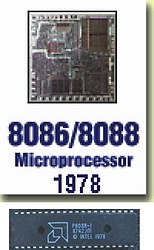 |
1982
i80286 announced. "286th" became the first x86 processor to penetrate the Soviet and post-Soviet space large quantity. Clocked at 6, 8, 10 and 12 MHz, it was manufactured using a 1.5-micron process technology and contained about 130,000 transistors. This chip had full 16-bit support. For the first time, with the advent of the i80286, such a concept as “protected mode” appeared, but then software developers did not use its capabilities to the fullest. The processor could address more than 1 MB of memory by switching to protected mode, but it was possible to return back after a full restart, and the segmented organization of memory access required significant additional effort when writing program code. This led to the fact that the i80286 was used more like a fast i8086.
 |
The performance of the chip compared to 8086 (and especially compared to i8088) increased several times and reached 2.6 million operations per second. In those years, manufacturers began to actively use the open architecture of the IBM PC. At the same time, the period of cloning of x86 architecture processors from Intel by third-party manufacturers began. That is, the chip was produced by other companies in the form of an exact copy. The Intel 80286 became the basis for the latest IBM PC/AT and its numerous clones. The main advantages of the new processor were increased performance and additional addressing modes. And most importantly - compatibility with existing software. Naturally, the processor was also licensed by third parties...
In the same year, AMD enters into a license agreement with Intel and, on its basis, begins production of clones of x86 processors.
1985
Perhaps the most significant event in the history of x86 processors took place this year - Intel released the first i80386 processor. It has become, one might say, revolutionary: a 32-bit multitasking processor with the ability to run multiple programs simultaneously. In fact, the most modern processors are nothing but fast 386s. Modern software uses the same 386 architecture, it's just that modern processors do the same thing, only faster. The Intel 386™ is a big improvement over the i8086 and i80286. In fact, the most modern processors are nothing but fast 386s. Modern software uses the same 386 architecture, it's just that modern processors do the same thing, only faster. The Intel 386™ is a big improvement over the i8086 and i80286. The Intel 386™ had significantly improved memory management over the i80286, and built-in multitasking enabled the development operating system Microsoft Windows and OS/2.
 |
Unlike the i80286, the Intel 386™ could freely switch from protected mode to real mode and back, and had a new mode, virtual 8086. In this mode, the processor could execute several different software threads at the same time, since each of them ran on an isolated "virtual" 86- th car. The processor introduced additional memory addressing modes with variable segment length, which greatly simplified the creation of applications. The processor was manufactured using a 1-micron manufacturing process. For the first time, the Intel processor was introduced with several models that formed the 386 family. This is where Intel's famous marketing game begins, which later resulted in the division of one developed core into two trading options, in a certain circle of users and specialists called: "Pentium for the rich, Celeron for the poor." Although what's wrong here - and the wolves are full, and the sheep are safe.
The following models were released:
The 386DX at 16, 20, 25 and 33 MHz had 4 GB of addressable memory;
386SX with a frequency of 16, 20, 25 and 33 MHz, unlike 386DX, had a 16, not a 32-bit data bus, and, accordingly, 16 MB of addressable memory (in a similar way, at one time, the i8088 processor was "created" from i8086 by external bus to ensure compatibility with existing external devices);
386SL in October 1990 - mobile version processor Intel 386SX with a frequency of 20 and 25MHz.
1989
Intel Corporation releases its next processor - Intel 486™ DX with a frequency of 25, 33 and 50 MHz. Intel 486 ™ DX was the first processor in the 486 family and had a significant (more than 2 times at the same frequency) performance increase compared to the 386 family. -cache increased to 512 Kb. The i486DX integrated a floating point unit (FPU - Floating Point Unit), which previously ran as an external math coprocessor installed on the motherboard. In addition, this is the first processor, the core of which contained a five-stage pipeline. Thus, the instruction that passed the first stage of the pipeline, continuing to be processed on the second, released the first for the next instruction. At its core, the Intel 486™DX processor was a fast Intel 386DX™ combined with a math coprocessor and 8K cache on a single die. Such integration allowed to increase the speed of communications between blocks to very high values.
Intel launched an advertising campaign with the slogan "Intel: The Computer Inside". Time will pass, and it will turn into the famous "Intel Inside" advertising campaign.
 |
1991
AMD's own processor, the Am386™, was created. This one was built partly under license, partly in-house, and ran at a maximum frequency of 40 MHz, which was higher than that of an Intel processor.
A little earlier, the first litigation between Intel and AMD took place over AMD's intention to sell its Intel 386™ clone. Having firmly strengthened its position, Intel no longer needed to distribute licenses to third-party manufacturers and was not going to share its own pie with anyone. As a result, AMD entered the x86 processor market for the first time as a competitor. Other companies followed. Thus began the ongoing great confrontation between the two giants (the rest of the competitors fell out of the race), which gave the world a lot of good. Unspoken slogan Intel competitors became the phrase: "the same as Intel, but at a lower price."
At the same time, Intel releases the i486SX, which lacks an FPU (integrated co-processor) to reduce the cost of the product, which, of course, negatively affected performance. There were no other differences from the i486DX.
 |
1992
With the release of the Intel 486DX2 processor, the bus frequency multiplier was used for the first time. Up to this point, the internal frequency of the core was equal to the frequency of the external data bus (FSB), but there was a problem of increasing it, since the local peripheral buses (at that time VESA VL-bus), and themselves peripherals showed instability at a frequency exceeding 33 MHz. Now, with a 33 MHz FSB, the core clock speed was 66 MHz due to multiplication by 2. This technique went down in history for a long time and is still used today, only the multiplier in modern CPUs can exceed 20. The Intel 486 ™ DX2 became a popular processor for a long time and was sold in huge quantities, however, as well as its clones from competitors (AMD, Cyrix and others), which now already had some differences from the “Intel original”.
 |
1993
The first superscalar x86 processor was released, that is, capable of executing more than one instruction per clock cycle - Pentium (codenamed P5). This was achieved by the presence of two independent parallel conveyors. The first processors had a frequency of 60 and 66 MHz and received a 64-bit data bus. For the first time, the first level cache was divided into two parts: separately for instructions and data. But one of the most significant innovations was a completely redesigned floating point unit (FPU). In fact, there had never been such a powerful FPU on the x86 platform before, and it was only many years after the release of the Intel Pentium that competitors were able to achieve its performance level. Also, for the first time, a branch prediction block was included in the processor, which has been actively developed by engineers since then.
The bottom line is this: in any program there are many conditional jumps, when, depending on the condition, the execution of the program must go one way or another. Only one of several transition branches can be placed in the pipeline, and if it turns out to be filled with the code of the wrong branch, then it has to be cleared and refilled for several cycles (depending on the number of stages of the pipeline). To solve this problem, branch prediction mechanisms are used. The processor contained 3.1 million transistors and was manufactured using a 0.8-micron process. All these changes made it possible to raise the performance of the new processor to an unattainable height. In reality, optimization of the code “for the processor” was rare at first and required the use of special compilers. And for a long time, the newest processor had to execute programs intended for processors of the 486 and 386 families.
In the same year, the second generation Pentium appeared on the P54 core, in which all the shortcomings of the P5 were eliminated. In the manufacture, new technological processes were used 0.6, and later 0.35-µm. Until 1996, the new processor covered clock frequencies from 75 to 200 MHz.
The first Pentium played an important role in the transition to new levels of personal computer performance, gave impetus and set the benchmarks for the development of the future. But with a big jump in performance, it did not bring any cardinal changes to the x86 architecture.
1994
The introduction of the Intel 486™DX4, AMD Am486DX4 and Cyrix 4x86 continued the 486 line and the use of data bus frequency multiplication. Processors had frequency tripling. Intel's DX4 processors ran at 75 and 100 MHz, while AMD's Am486DX4 reached 120 MHz. The power management system has become widely used in processors. No other fundamental differences from 486DX2 were found.
1995
Announced Pentium Pro (P6 core). New processor bus, three independent pipelines, optimization for 32-bit code, from 256 Kb to 1 Mb L2 cache integrated into the processor, and running at the core frequency, improved branch prediction mechanism - by the number of innovations new processor almost beat the records previously set by Intel Pentium.
 |
The processor was positioned for use in servers and had a very high price. The most remarkable thing is that the Pentium Pro computing core was not actually an x86 core. The x86 machine codes coming into the CPU were internally decoded into RISC-like microcode, and it was this microcode that was executed by the processor core. The CISC instruction set, like the x86 processor instruction set, implied a variable length of instructions, which made it difficult to find each individual instruction in the stream and, therefore, created difficulties in program development. CISC commands are complex and complex. RISC instructions are simplified, short, requiring much less time to execute a fixed length instruction. The use of RISC instructions allows you to significantly increase the parallelization of processor calculations, that is, use more pipelines and, consequently, reduce the execution time of instructions. The P6 core formed the basis of the next three Intel processors - Pentium II, Celeron, Pentium III.
A significant event also took place this year - AMD bought NexGen, which by that time had advanced architectural developments. The merger of the two engineering teams would later bring x86 processors to the world with a different microarchitecture from Intel and kick-start a new round of fierce competition.
Cyrix's new MediaGX processor was unveiled for the first time at the Microprocessor Forum, featuring an integrated memory controller, graphics accelerator, PCI bus interface, and Pentium-like performance. It was the first attempt at such a dense integration of devices.
1996
A new AMD K5 processor with a superscalar RISC core has appeared. However, the RISC core with its instruction set (ROP instructions) is hidden from the software and the end user, and the x86 instructions are converted to RISC instructions. AMD engineers used a unique solution - x86 instructions are partially converted while they are placed in the processor's cache memory. Ideally, the K5 processor can execute up to four x86 instructions per cycle, but in practice, on average, only 2 instructions are processed per cycle.
 |
In addition, traditional RISC processor reordering, register renaming, and other "tricks" can improve performance. The K5 processor was the brainchild of a joint team of AMD and NexGen engineers. The maximum clock speed never exceeded 116 MHz, but the performance of the K5 was higher than that of Pentium processors with the same clock speed. Therefore, for marketing purposes, for the first time in the practice of marking CPUs, a performance rating (Performance Rating) was used, which was clearly opposed to the clock frequency of Pentiums equal in performance. But the processor still could not adequately compete with it, since the Pentium had already reached a frequency of 166 MHz.
In the same year saw the release of the Intel Pentium MMX. The main innovation of the P55C processor is the additional MXX instructions to the instruction set, which has hardly changed since the creation of the third generation processors. MMX technology is the use of multimedia-oriented commands. A special set of SIMD commands (Single Instruction - Multiple Data - one command - multiple data) improves performance when executing vector, cyclic commands and processing large data arrays - when applying graphic filters and various special effects.
 |
In fact, these are 57 new instructions designed to speed up the processing of video and sound. The rest of the changes in the core were the typical increase in the amount of cache memory, improved schemes for the operation of the cache memory and other blocks. The processor was produced using a 0.35-micron process, 4.5 million transistors. The maximum frequency is 233 MHz.
The production of Cyrix 6x86 superscalar processors on the M1 core began, which was actually a 5th generation processor, the distinguishing feature of which was "deep" pipelines and the use of classic x86 instructions without any additional instruction sets.
At the end of the year, while Intel was developing the Pentium II, AMD again announced itself with the release of the sixth generation K6 processor. The AMD-K6 is based on the core developed by NexGen engineers for the Nx686 processor and significantly improved by AMD. Like K5, the K6 core did not operate on x86 instructions, but on RISC-like microcode. The processor supported MMX commands and a 100 MHz system bus and had an increased L1 cache to 64 KB. It soon became clear that the PentiumII would be too tough for the K6.
from 1997 to today...
By 1997, the directions of engineering development of the x86 architecture of the leading manufacturers had already taken shape. The next stage in the development of x86 processors can be described as a confrontation between architectures, which continues to this day. They have come a long way: Intel, which has captured 90% of the market, AMD is stubbornly fighting with it, losing many times in production capacity, and Cyrix, which will later be bought by VIA, and then completely, unable to withstand the competition, will sink into obscurity. Other manufacturers will not be able to compete adequately and will be forced to look for other niches in the market. A transition from CISC to RISC-like microinstructions is planned, to a lesser extent at Intel, to a greater extent at AMD. Moreover, CISC commands are still received at the input and output of x86 processors. And why, in fact, did x86 processors with their native CISC architecture begin to introduce an internal RISC architecture that allows deepening the parallelization of instruction execution? Yes, just from the x86 CISC architecture back in the days fourth generation everything was squeezed out, and there were no ways to improve performance at the level of basic instruction sets.
 |
There have been no fundamentally new changes and breakthroughs in the development of architecture since then, although modern processors are hundreds of times faster, for example, the 386th. Engineers hone and improve the existing microarchitectures of the cores, and the new ones are just reworked old ones. All improvements and attempts to improve performance come down to optimizing existing solutions, introducing various fixes and “crutches” for lame FPUs, pipelines and caches. A hackneyed, but still effective means is a constant increase in the amount of cache memory and the frequency of the FSB bus. Modern processors have up to 2 MB of cache memory running at the core frequency, and the frequencies system buses reach 800 MHz, and then using a multiplier, since the real generated frequency is only 200 MHz. Over the past 7 years, the following “support innovations” have been introduced into x86 processors: cache memory has finally moved to the processor chip and transferred to the core frequency, branch prediction units have been introduced and are constantly being improved as compensation for an increase in the length (number of stages) of the pipeline, a dynamic change mechanism order of execution of instructions, which reduces the number of idle cycles, a data prefetch mechanism for more rational use of cache memory. Additional command sets are multiplying: SSE, SSE2, SSE3, 3DNow!, 3DNow Professional. If MMX could still be called an additional set of x86 instructions with a stretch, then all subsequent sets are unlikely, since there is nothing to add to the x86 commands. The meaning of the appearance of these sets is to try to use the floating point unit (FPU) as little as possible in the form in which it exists, since, having high performance, it is not very adaptable for high-precision calculations, the capriciousness of the internal architecture and its unpredictability , which makes life difficult for programmers. That is, in fact, a specialized calculation unit was introduced, focused not on calculations in general, but on real, frequently occurring tasks, which are proposed to be performed bypassing the classic FPU.
 |
Somehow it looks more like dealing with the consequences of integrating a math coprocessor into the CPU back in 1989. In any case, if you think about it and calculate, then the processor spends most of its time “on itself” - on all kinds of transformations, predictions, and much more, and not on executing program code.
Looking back, it is clear that not everything went smoothly. The introduction of a multiplication factor and the resulting asynchrony, as well as an increase in the number of pipeline stages, are all double-edged swords. On the one hand, this allowed us to increase the processor clock speeds to almost 4 GHz (and this is not the limit), on the other hand, we got a bottleneck in the form of the FSB bus and a problem with conditional jumps. But everything has its time, and then, apparently, these were reasonable decisions, since there is always a very evil economic factor.
It should be noted that truly brilliant successes have been achieved in recent years in the field of semiconductor production. The 90-nm technological process for manufacturing x86 processors has already been mastered, which allows reaching close to the microwave range clock frequencies, and the number of transistors in a crystal reaches 170 million (Pentium 4 EE).
We are used to thinking that the processor is the main device in the PC and that it is he who sets the tone for global computing. But the victorious march of the x86 architecture, lasting more than a quarter of a century, began not specifically with the processor, but with the end user device as a whole - the IBM PC. At that time, even at IBM, they had no idea what a brilliant future awaited this PC and, without attaching any importance to the project, made it open to everyone. It is the openness of the concept, the success of software and MS DOS that owes the success of the IBM PC. And the processor in it could be of any architecture, but it just so happened that IBM chose the i8088 and i8086, and then everything started spinning, spinning ... But the x86 processor did not end up with such a universal calculator for all occasions or a "smart" device, ubiquitous and able to do everything as it was dreamed of before. And Gordon Moore's "law" (every 2 years the number of transistors in a processor chip will double) became a law only for Intel, which put it at the forefront of its marketing policy, and apparently it is inconvenient for her to refuse this word.
 |
Today we can already firmly say that the x86 architecture has reached a dead end. Its contribution to the popularization of the computer as a device is enormous, and no one argues with that. However, you can't be up to date forever. The once young and strong stallion has become an old horse, which they continue to harness to the cart. The appetites of users are insatiable, and soon the x86 architecture will not be able to satisfy them. Of course, the transition is associated with titanic efforts due to the fact that the multimillion-strong global PC fleet in its almost absolute majority uses x86 architecture processors, and, most importantly, uses software for x86 code. You can't change everything in one day, it takes years. But the development of 64-bit processors and programs is gaining momentum at an enviable rate, Intel has introduced Itanium2, and AMD has been releasing its Athlon 64 for almost a year now, which do not have x86 architecture at all, although they are fully compatible with it and can still run all old programs. Thus, we can say that AMD Athlon 64 marked the beginning of the departure from the x86 architecture and thus opened the transition period.
As you can see, claims that the processor is the fastest growing PC component are far from groundless. Imagine what kind of processors our children's computers will be equipped with. Think scary!
 |
In Odnoklassniki